
LM3644EVM
具有 1.5A 高侧电流源的同步升压双路 LED 闪存驱动器评估模块
1 Introduction
The Texas Instruments LM3644EVM evaluation module (EVM) helps designers evaluate the operation and performance of the LM3644 High-Current LED driver. The device offers configurability via I2C compatible interface. It can be enabled in Flash or Torch mode via the I2C interface or externally using the STROBE and TORCH/TEMP pins. The module utilizes two LEDs (D1 & D2) mounted on the EVM.
2 Setup
This section describes the jumpers and connectors on the EVM as well as how to properly connect, set up, and use the LM3644EVM.
2.1 Input/Output Connector Description
Input / GND- These are the power input terminals for the driver. The terminal block provides a power (VIN) and ground (GND) connection to allow the user to attach the EVM to a cable harness.
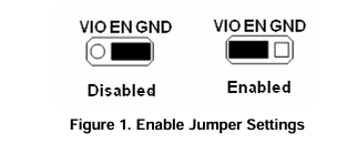
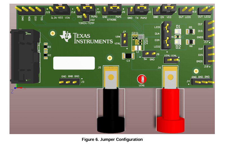
EN (J12)- This is the jumper used to enable the LED driver (HWEN pin). The driver will be enabled when the HWEN pin is high (VIO) and disabled when it is low (GND).
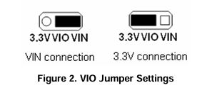
VIO (J16)- This pin provides power for the I2C lines (Clock & Data) and for the HWEN pin. It is recommended that this pin is connected to the VIN pin. If desired, it can be connected to the 3.3V line provided by the USB interface connector. In this configuration, communication via the I2C interface may not be possible if the supply voltage to the LED driver is below approximately 3 V.
D1-CON (J14 pin3 and pin4) and D2-CON (J14 pin1 and pin2) are the jumpers used to connect the on board flash LEDs to the LED output of the driver.
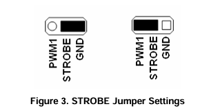
STROBE (J9)- This pin provides an external method for initiating a flash event. The STROBE pin is connected to ground via a 300-kΩ resistor internal to the LM3644. To externally drive this pin, either connect a control signal directly to the STROBE pin of the connector or place a jumper between connector pins STROBE and PWM0. Pin PWM0 can be configured as a time-adjustable voltage pulse via the General User Interface (GUI) software provided.
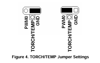
TORCH/TEMP (J21)- This pin provides an external method for initiating a torch event. The TORCH/TEMP pin is connected to ground via a 300-kΩ resistor internal to the LM3644 as well as an externally connected NTC thermistor. To externally drive this pin, either connect a control signal directly to the TORCH/TEMP pin of the connector or place a jumper between connector pins TORCH/TEMP and PWM1. Pin PWM1 can be configured as ON or OFFvia the GUI software provided. Removing the jumper, and setting the TORCH/TEMP pin to TEMP mode, the TEMP function can be utilized via the externally connected NTC thermistor.
TX (J11)- This pin is used to initiate a TX-interrupt event. The TX pin is connected to ground via a 300-kΩ resistor internal to the LM3644. To externally drive this pin, either connect a control signal directly to the TX pin of the connector or place a jumper between connector pins TX and PWM2. Pin PWM2 can be configured as to provide continuous voltage pulses via the GUI software provided.
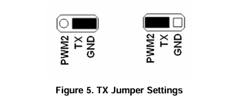
SDA / SCL (J19)- These connections allow the user to externally control the I2C lines. For independent control of the I2C lines, do not connect the VIO jumper to either the 3.3 V or the VIN pin.
OUT, LED1, LED2, TORCH/TEMP (J13, J10, J22)- These provide access to the regulated output of the driver, the outputs of the LED current sources, and the TEMP pin. The user can measure VOUT with reference to GND, VLED with reference to GND, current source headroom directly between VOUT and VLED, and can monitor or control TORCH/TEMP input.
VINL/VIN (J7)- The user can monitor the Inductor Current and Input Current waveforms by omitting this jumper and using separate wires from the power supply to the VINL and VIN pins. This will remove the Input Capacitors from the Inductor and eliminate their filtering effect to the Inductor Current.
J17 and J18: LED Current measurements-The LM3644EVM provides a way to accurately measure the LED current through both LEDs on board. Resistors R1 & R2 (0.1 Ω) are placed between the cathode of LED1 & LED2, respectively, and Ground. The user can first measure the resistor values accurately, by applying a known current through connector DxF and Ground and measuring the voltage between DxS and GNDS. Then, during normal flash or torch operation, the voltage measured across the resistor divided by the resistor value will equal the current through the resistor (and the LED).
2.2 Setup
The input voltage range for the flash driver is 2.5 volts to 5.5 volts. The on-board LEDs or an LED module should be connected for proper operation.
2.3 Operation
For proper operation of the LM3644EVM, the jumpers should be properly configured. The recommended setting, using shorting blocks is:
VIO to VIN
EN to VIO
STROBE to PWM0 or external signal
TORCH/TEMP to PWM1 or external signal
TX to PWM2 or external signal
LEDs (J14) shorted
In this configuration, the device will power up when power is applied
3 Board Layout
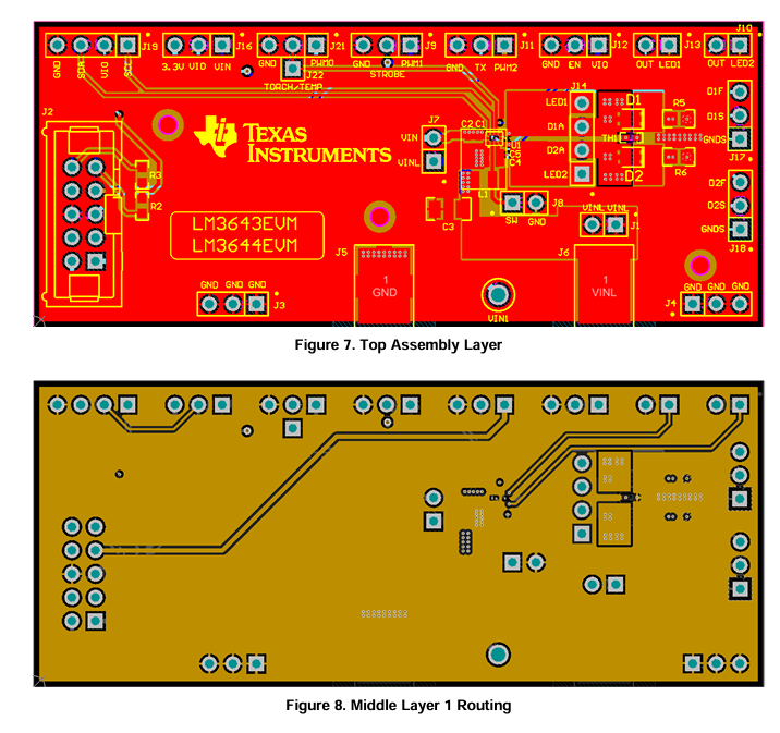
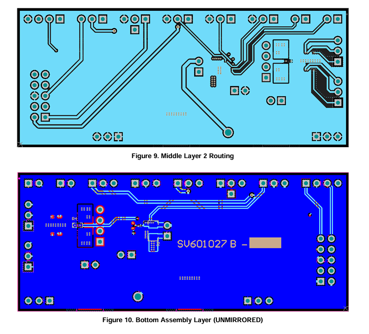
Figure 7, Figure 8, Figure 9 and Figure 10 show the board layout for the LM3644EVM. The EVM offers resistors, capacitors, and jumpers to enable the device and to configure it as desired.
The LM3644 will dissipate power, especially during high current and long duration flash events. Power will also be dissipated on the flash LEDs. The EVM layout is designed to minimize temperature rise during operation. It is recommended that in order to prevent overheating, repeated flash events in very short time intervals is avoided.
4 Schematic
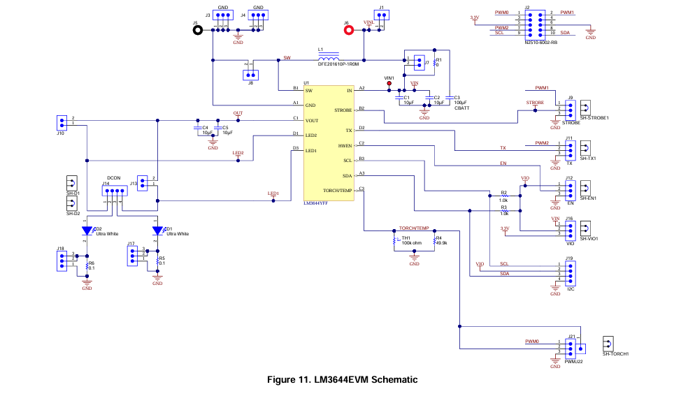
- TLA2024EVM-PDK_TI(德州仪器)中文资料_英文资料_价格_PDF手册
- INA229_239EVM_TI(德州仪器)中文资料_英文资料_价格_PDF手册
- DAC8832EVM-PDK _TI(德州仪器)中文资料_英文资料_价格_PDF手册
- LP8557IEVM_TI(德州仪器)中文资料_英文资料_价格_PDF手册
- LAUNCHXL-F28027F TI(德州仪器)中文资料_英文资料_价格_PDF手册
- DLPDLCR160CPEVM DLP160CP TI(德州仪器)中文资料_英文资料_价格_PDF手册
- THS4631DDAEVM TI(德州仪器)中文资料_英文资料_价格_PDF手册
- DAC3482EVM TI(德州仪器)中文资料_英文资料_价格_PDF手册
- THS4302EVM TI(德州仪器)中文资料_英文资料_价格_PDF手册
- ADS7038Q1EVM-PDK_TI(德州仪器)中文资料_英文资料_价格_PDF手册
- LM3450AEV230V30/NOPB_TI(德州仪器)中文资料_英文资料_价格_PDF手册
- TPS72728DSEEVM-406_TI(德州仪器)中文资料_英文资料_价格_PDF手册
- WL1835MODCOM8A_TI(德州仪器)中文资料_英文资料_价格_PDF手册
- TAS5424BQ1DKDEVM_TI(德州仪器)中文资料_英文资料_价格_PDF手册
- ADS7042EVM-PDK_TI(德州仪器)中文资料_英文资料_价格_PDF手册
 工商网监
工商网监