TPS72728DSEEVM-406
EVAL MODULE FOR TPS72728DSE-406
This User’s Guide describes the characteristics, operation, and use of the TPS727xxDSEEVM-406. This EVM demonstrates the Texas Instruments TPS727xx, a Low Drop Out (LDO) linear regulator in a 1,5 × 1,5mm SON-6 package that is capable of 200mA of output current. This user’s guide includes setup instructions, a schematic diagram, thermal guidelines, a bill of materials (BOM), and PCB layout drawings for the evaluation module
1 Introduction
The TPS727xxDSEEVM-406 evaluation module (EVM) helps designers evaluate the operation and performance of the TPS727xx LDO in the 1,5 × 1,5mm SON-6 package. The TPS727xx is a 200mA, ultra-low Iq, fast transient response, linear regulator.
2 Setup
This chapter describes the jumpers and connectors on the EVM as well as how to properly connect, setup, and use the TPS727xxEVM.
2.1 Input / Output Connector Descriptions
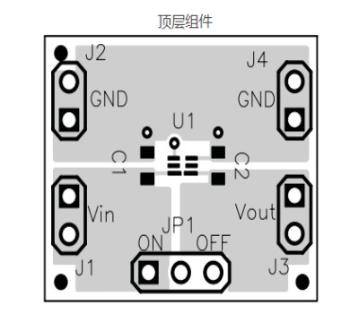
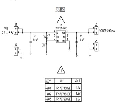
2.1.1 J1 –VIN
This is the positive input supply voltage. The leads to the input supply should be twisted and kept as short as possible to minimize EMI transmission. Additional bulk capacitance should be added between J1 and J3 if the supply leads are greater than six inches. An additional 47µF or greater capacitor improves the transient response of the TPS727xx and helps to reduce ringing on the input when long supply wires are used.
2.1.2 J3 – VOUT
This is the positive connection from the output. Connect this pin to the positive input of the load.
2.1.3 J2 – GND
This is the return connection for the input power supply of the regulator
2.1.4 J4 – GND
This is the return connection for the output
2.1.5 JP1 – ENABLE
This jumper is used to enable or disable the output of the TPS727xx. Placing a shorting jumper between pins 1 and 2 (‘ON’ position) will enable the TPS727xx. Placing the shorting jumper between pins 2 and 3 (‘OFF’ position) will disable the TPS727xx.
3 Operation
This chapter provides information about the operation of the TPS727xxEVM.
3.1 Operation
Connect the positive input power supply to J1. Connect the input power return (ground) to J2. The TPS727xxEVM has an absolute maximum input voltage of 6.0V. The recommended maximum operating voltage is 5.5V. The actual highest input voltage may be less than 5.5V due to thermal conditions. See the Thermal Considerations section of this manual to determine if the highest input voltage.
Connect the desired load between J3 (positive lead) and J4 (negative or return lead). Configure jumper J6 for the desired output voltage.
4 Thermal Guidelines
This chapter provides guidelines for the thermal management of the TPS727xxDSEEVM-406 board.
4.1 Thermal Considerations
Thermal management is a key component of design of any power converter and is especially important when the power dissipation in the LDO is high. To better help you design the TPS727xx family into your application, the following formula should be used to approximate the maximum power dissipation at a particular ambient temperature:
TJ = TA + Pd × θJA
Where
TJ is the junction temperature
TA is the ambient temperature,
Pd is the power dissipation in the IC and
θJA is the thermal resistance from junction to ambient.
All temperatures are in degrees Celsius.
The measured thermal resistance from junction to ambient for the TPS727xxEVM has a typically value of 130°C/W. The recommended maximum operating junction temperature specified in the datasheet for the TPS727xx family is 125°C. With these two pieces of information, the maximum power dissipation can be found by using Equation 1
Example Calculation:
For example, what is the maximum input voltage that can be applied to a TPS727xx with a 1.5V output voltage if the ambient temperature is 85°C and the full 200mA of load current is required?
Given: TJ = 125°C, TA = 85°C, θJA = 130°C/W
Using Equation 1, we substitute in the given values above and find that the maximum power dissipation for the part is Pd = 0.307W.
125°C = 85°C + Pd (130°C/W)
This means that the total power dissipation of the TPS727xx must be less than 0.833W. Now the input voltage can be calculated.
Pd = (Vin – Vout) × I out = (Vin – 1.5V) × 0.2A = 0.307W
the maximum input voltage would need to be 3.04V or less in order to maintain a safe junction temperature.
Similar analysis can be performed to determine the maximum input voltage at room temperature (25°C) or 85°C to provide full output current while maintaining the junction temperature at or below 125°C. The answer will depend on the output voltage.
5 Board Layout
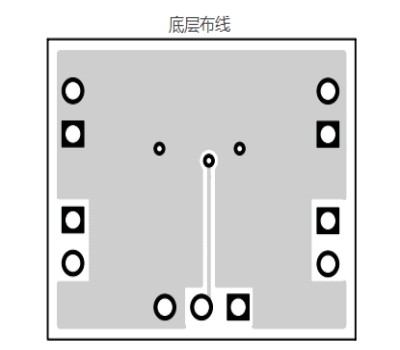
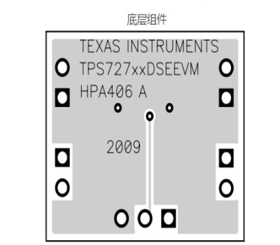
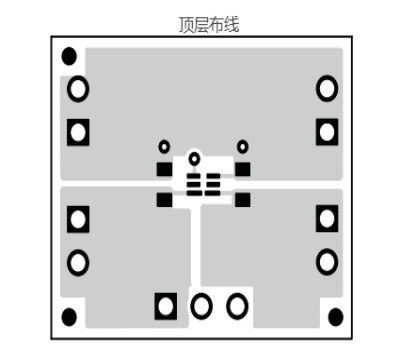
This chapter provides the TPS727xxDSEEVM-406 board layout and illustrations
5.1 Layout
6 Schematic and Bill of Materials
This chapter provides the TPS727xxDSEEVM-406 schematic and bill of materials.
6.1 Schematic
- LP8557IEVM_TI(德州仪器)中文资料_英文资料_价格_PDF手册
- LAUNCHXL-F28027F TI(德州仪器)中文资料_英文资料_价格_PDF手册
- DLPDLCR160CPEVM DLP160CP TI(德州仪器)中文资料_英文资料_价格_PDF手册
- THS4631DDAEVM TI(德州仪器)中文资料_英文资料_价格_PDF手册
- DAC3482EVM TI(德州仪器)中文资料_英文资料_价格_PDF手册
- THS4302EVM TI(德州仪器)中文资料_英文资料_价格_PDF手册
- ADS7038Q1EVM-PDK_TI(德州仪器)中文资料_英文资料_价格_PDF手册
- LM3450AEV230V30/NOPB_TI(德州仪器)中文资料_英文资料_价格_PDF手册
- TPS72728DSEEVM-406_TI(德州仪器)中文资料_英文资料_价格_PDF手册
- WL1835MODCOM8A_TI(德州仪器)中文资料_英文资料_价格_PDF手册
- TAS5424BQ1DKDEVM_TI(德州仪器)中文资料_英文资料_价格_PDF手册
- ADS7042EVM-PDK_TI(德州仪器)中文资料_英文资料_价格_PDF手册
- TMDS570LS31HDK_TI(德州仪器)中文资料_英文资料_价格_PDF手册
- VCA8500BOARD_TI(德州仪器)中文资料_英文资料_价格_PDF手册
- DEM-SOT223LDO_TI(德州仪器)中文资料_英文资料_价格_PDF手册
