
TLV7163318PEVM-535
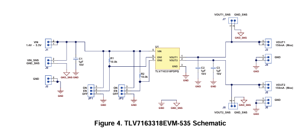
This User’s Guide describes the operational use of the TLV7163318PEVM-535 Evaluation Module (EVM) as a reference design for engineering demonstration and evaluation of the TLV7163318P, dual low dropout linear regulator (LDO). Included in this user’s guide are setup instructions, a schematic diagram, layout, thermal guidelines, a bill of materials, and test results.
1 Introduction
The Texas Instruments TLV716xxxxEVM-535 EVM helps design engineers to evaluate the operation and performance of the TLV716xxxx family of dual linear regulators for possible use in their own circuit application. This particular EVM configuration contains a dual linear regulator with low IQ , and possible cap free operation in a small 1.2 mm x 1.2 mm DPQ package. Each regulator is capable of delivering up to 150 mA to the load depending on the input-output power dissipation across the part which can be minimized because of the low dropout voltage.
2 Setup
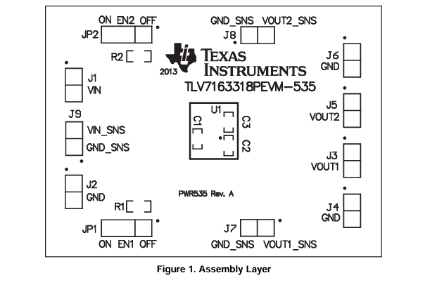
This section describes the jumpers and connectors on the EVM as well as how to properly connect, setup, and use the TLV7163318EVM-535.
2.1 Input/Output Connectors and Jumper Descriptions
2.1.1 J1– VIN
Input power supply voltage connector. Twist the positive input lead and ground return lead from the input power supply and keep them as short as possible to minimize EMI transmission. Add additional bulk capacitance between J1 and J2 if the supply leads are greater than six inches. For example, an additional 47 µF electrolytic capacitor connected from J1 to ground can improve the transient response of the TLV7163318 while eliminating unwanted ringing on the input due to long wire connections.
2.1.2 J2– GND
Return connector for the input power supply.
2.1.3 J3– VOUT1
Regulated output voltage connector of LDO1.
2.1.4 J4– GND
Output ground return connector of LDO1.
2.1.5 J5– VOUT2
Regulated output voltage connector of LDO2.
2.1.6 J6– GND
Output ground return connector of LDO2.
2.1.7 J7– VOUT1_SNS/GND_SNS
VOUT1_SNS/GND_SNS are the sense connection for the output of LDO1. Connect a voltmeter, sense connection of an electronic load, or oscilloscope to this header.
2.1.8 J8– VOUT2_SNS/GND_SNS
VOUT2_SNS/GND_SNS are the sense connection for the output of LDO2. Connect a voltmeter, sense connection of an electronic load, or oscilloscope to this header.
2.1.9 J9– VIN_SNS/GND_SNS
VIN_SNS/GND_SNS are the sense connection for the input of LDO1 and LDO2. Connect a voltmeter, sense connection of an electronic load, or oscilloscope to this header.
2.1.10 JP1– EN1
Output enable of LDO1. To enable the output, connect a jumper to short the VIN pin 3 to the EN center pin 2. To disable the output, connect a jumper to short EN pin 2 to GND pin1. EN is pulled up to VIN through resistor R1 when JP1 is not connected.
2.1.11 JP1– EN2
Output enable of LDO2. To enable the output, connect a jumper to short the VIN pin 3 to the EN center pin 2. To disable the output, connect a jumper to short EN pin 2 to GND pin1. EN is pulled up to VIN through resistor R1 when JP2 is not connected.
2.2 Soldering Guidelines
Any solder re-work to modify the EVM for the purpose of repair or other application reasons must be performed using a hot-air system to avoid damaging the integrated circuit (IC).
2.3 Equipment Interconnect
• Set the input power supply to 5.5V(max). Turn the power supply off. Connect the positive voltage lead from input power supply to VIN, at the J1 connector of the EVM. Connect the ground lead from the input power supply to GND at the J2 connector of the EVM.
• Connect a 0- 150 mA load between VOUT1, at connector J3, and GND, at connector J4.
• Connect a 0- 150 mA load between VOUT2, at connector J5, and GND, at connector J6.
• Disable the output by jumping JP1 and JP2, the EN pin to the OFF pin.
3 Operation
• Turn on the power supply.
• Enable the output by jumping JP1 and JP2, the EN pin to the ON pin.
• Vary the respective load and input voltage as necessary for test purposes
4 Thermal Guidelines and Layout Recommendations
Thermal management is a key component of design of any power converter and is especially important when the power dissipation in the LDO is high. Use the following formulas to approximate the maximum power dissipation for the particular ambient temperature:
TJ = TA + PD x θJA
PD = (VIN- VOUT1 ) × IOUT1 + (VIN- VOUT2 ) × IOUT2
Where TJ is the junction temperature, TA is the ambient temperature, PD is the power dissipation in the device (Watts), and θJA is the thermal resistance from junction to ambient. All temperatures are in degrees Celsius. The maximum operating junction temperature, TJ, must not be allowed to exceed 125°C. The layout design must be copper trace and plane areas smartly, as thermal sinks, in order not to allow TJ to exceed the absolute maximum rating under all temperature conditions and voltage conditions across the part.
Table 1 repeats information from the Dissipation Ratings Table of the TLV7163318 series data sheet for comparison with the thermal resistance, θJA , for High-K JEDEC standard boards. The maximum input voltage can be calculated for full loads at different ambient temperatures. The input voltage must be less than these values in order to maintain a safe junction temperature.

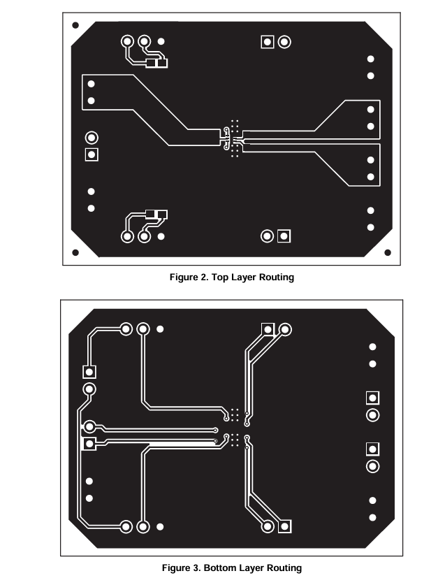
5 Board Layout
6 Schematic
- 苏州杭晶电子入驻工之芯商城,成为优质供应商
- TPS7A30-49EVM-567_TI(德州仪器)中文资料_英文资料_价格_PDF手册
- TLA2024EVM-PDK_TI(德州仪器)中文资料_英文资料_价格_PDF手册
- INA229_239EVM_TI(德州仪器)中文资料_英文资料_价格_PDF手册
- DAC8832EVM-PDK _TI(德州仪器)中文资料_英文资料_价格_PDF手册
- LP8557IEVM_TI(德州仪器)中文资料_英文资料_价格_PDF手册
- LAUNCHXL-F28027F TI(德州仪器)中文资料_英文资料_价格_PDF手册
- DLPDLCR160CPEVM DLP160CP TI(德州仪器)中文资料_英文资料_价格_PDF手册
- THS4631DDAEVM TI(德州仪器)中文资料_英文资料_价格_PDF手册
- DAC3482EVM TI(德州仪器)中文资料_英文资料_价格_PDF手册
- THS4302EVM TI(德州仪器)中文资料_英文资料_价格_PDF手册
- ADS7038Q1EVM-PDK_TI(德州仪器)中文资料_英文资料_价格_PDF手册
- LM3450AEV230V30/NOPB_TI(德州仪器)中文资料_英文资料_价格_PDF手册
- TPS72728DSEEVM-406_TI(德州仪器)中文资料_英文资料_价格_PDF手册
- WL1835MODCOM8A_TI(德州仪器)中文资料_英文资料_价格_PDF手册
 工商网监