
ADS7864M-EVM
EVAL MODULE FOR ADS7864M
This user's guide describes the characteristics, operation, and use of the ADS7864MEVM 12-bit parallel analog-to-digital converter evaluation module. A completecircuitdescription,aschematicdiagram,andbillofmaterialsareincluded.
1 EVMOverview
1.1 Features
• Full-featuredevaluationboardfortheADS7864250-KHz,16-bit,6-channelsimultaneoussampling analog-to-digitalconverter
• Analoginputscanbeconfiguredassingle-endedordifferential
• ModularEVMformatallowsconnectiontoC5000™andC6000™DSKplatformsthroughthe5-6K InterfaceBoard.
• Built-inreference
• High-speedparallel interface
2 Introduction
The ADS7864 contains two high-speed 12-bit A/D converters that operate from independent +5-V Avdd and Dvdd supplies. Each A/D in the chip is preceded by a 3:1 multiplexer, providing six total input channels. The parallel digital output is provided as a 16-bit word which contains both channel address information and conversion data results.
Each of the six input channels contains a fully differential sample-and-hold circuit arranged into three pairs (A, B, and C). Each channel pair has a hold signal (HOLDA, HOLDB, and HOLDC) which, when strobed together, allows simultaneous sampling of all six analog inputs. The device accepts an analog input voltage in the range of–VREF to +VREF. The ADS7864 also accepts bipolar input ranges when a level shift circuit is used in the analog front-end circuitry (see Figure 1).
Conversion time for the ADS7864 is 1.75 µs when an 8-MHz external clock is used. The corresponding acquisition time is 0.25 µs. To achieve maximum output rate (500 kHz), the read function can be performed at the start of the next conversion cycle.
3 Analog Interface
The analog input to the ADS7864 is divided in two parts. Connector J4 provides access to input channels A1 and B1 through two different amplifier circuit configurations. The input buffer configuration of channel A1 presents a typical front-end circuit for the A/D converter. Its function is to provide level and impedance adaptation of the input signal. The input to channel B1 is a bipolar configuration using the INA159 to accommodate ±10-V input signals. Connector J3 provides access to the remaining analog input channels through a simple R/C filter.
3.1 Analog Input– Channel A1
The analog input to the ADS7864MEVM board for channel A1 is comprised of the dual OPA2132 operational amplifier and the associated circuitry as shown in Figure 1. The OPA2132 is powered from the ±12-V analog supply, and arranged as an inverting amplifier with a gain of 1. The internal +2.5-V reference voltage of the ADS7864 is applied to the noninverting input of the OPA2132 to provide input bias.
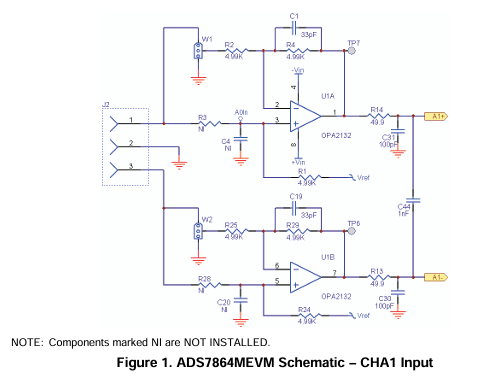
This configuration allows single-ended signals of ±2.5-V (+5-Vpp) to be applied to either the (+) or (-) input of channel A1 (via J2 pin 1 or 3 referenced to pin 2). The input also can be applied to connector J4 (not shown) pins 2 or 4, referred to analog ground.
3.2 Bipolar Input to Channel A1
By changing resistor components and setting the appropriate jumpers, it is possible to configure the input buffer to accept bipolar input voltages. Table 1 is related to the schematic presented in Figure 1 and represents just a few of the possible input configurations.
The output from the buffer stage in each case applies 0 V to 5 V to the CHA1(+) input when the applied signal is connected to J2 pin 1 or J4 pin 2. The applied signal is directed to the CHA1(-) input when connected via J2 pin 3 or J4 pin 4.
When operating the ADS7864 with single-ended signals it is important to keep the unused ADC input biased to +2.5 V. This is easily accomplished on the EVM by changing the components associated with either the inverting or noninverting only, leaving the default component values shown above on the unused input. For example, to achieve a bipolar input range of ±10 V on CHA1(+), use the component values shown above for R1–R4 and move the shunt on W2 from position 1-2 to position 2-3. Components R24, R25, R28, and R29 and the shunt on W1 should remain in the default conditions shown in Table 1
3.3 Analog Input– Channel B1
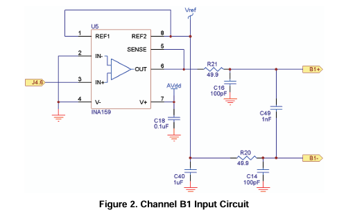
The analog input to the ADS7864MEVM board for channel B1 is comprised the INA159 difference amplifier and the associated circuitry as shown in Figure 2. The INA159 is powered from the +5-V analog supply, and arranged as a noninverting amplifier with a gain of 0.2. The internal +2.5-V reference voltage of the ADS7864 is applied to both REF1 and REF2 pins of the INA159 to provide a direct ±10-V interface with built-in level translation to the noninverting input of channel B1.
3.4 Analog Inputs–Channels A0, B0, and C1/C0
The analog inputs to the remaining ADS7864 input channels are routed to connector J3 and configured with simple R/C filters only. This configuration allows the EVM user to apply any customized input circuit to the data converter. Connector J3 is comprised of a male/female pass-through combination of pin header and socket with industry standard 0.1-inch centers.
When the ADS7864MEVM is used in combination with the 5-6K Interface Board or HPA-MCU Interface board, the DAP Signal Conditioning Board (SLAU105 ) can be used to drive the remaining input channels.
4 Digital Interface
The ADS7864MEVM is designed for easy interfacing to multiple control platforms. Jumper options are provided on the EVM to allow control over the state of Chip Select pin (CS) as well as the operating mode pins (A0–A2) the Reset pin (RST) and the Conversion Start strobes (HOLDA, HOLDB, and HOLDC).
Jumpers W4 and W6 control the signals applied to A0, A1, A2 and CS. In the factory default mode, W6 is closed by means of a shunt jumper. The Ax and CS pins are controlled by the signals applied to J5 (top or bottom side). When used with either the 5-6K or HPA-MCU Interface Boards, these control signals are associated with the host processors address bus.
By removing the shunt jumper located at W6, the A0, A1, and A2 pins are controlled by shunt jumpers placed on W4. The CS pin is routed to J5.1, which requires the application of an active-low Chip Select signal. A simple shunt jumper placed across J5 pins 1-2 can be used to force the CS pin to ground if desired.
4.1 Parallel Control
Samtec part numbers SSW-110-22-F-D-VS-K and TSM-110-01-T-DV-P provide a convenient 10-pin dual-row header/socket combination at J5 (Table 2). This header/socket provides access to the digital control pins of the EVM. Consult Samtec at www.samtec.com or 1-800-SAMTEC-9 for a variety of mating connector options.
4.2 Parallel Data
The ADS7864MEVM uses Samtec part numbers SSW-116-22-F-D-VS-K and TSM-116-01-T-DV-P provide a convenient 16-pin, dual-row, header/socket combination at J6. This header/socket combination provides access to the parallel data pins of the ADS7864. Data line D0 is connected to J6 pin 1. Data lines 1–15 are located on pins 3–31, respectively. Even pin numbers 2–32 are connected to digital ground
4.3 GPIO/Control Options
Samtec part numbers SSW-110-22-F-D-VS-K and TSM-110-01-T-DV-P also provide a 10-pin, dual-row header/socket combination at J1 to facilitate general-purpose input/output (GPIO) control options to the ADS7864. Table 3 describes the functions and pinout of J1
5 Power Supplies
The ADS7864MEVM board requires +5 VDC for the both the analog and digital section of the ADC. The supply (+Va and +Vd) can range from +4.75 VDC to +5.25 VDC. Because the EVM is designed to work with the 5-6K and HPA-MCU Interface Boards, JP1 provides direct connection to the common power bus described in SLAU104 . Table 4 shows the pinout of JP1:
Alternate power sources can be applied through various test points located on the EVM. See the schematic at the end of this document for details. Note– although filters are provided for all power supply inputs, optimal performance of the EVM requires a clean, well-regulated power source.
5.1 Reference Voltages
The ADS7864MEVM is configured to use its internal reference through jumper W3 (see schematic for details). If an external reference is desired, the shunt jumper on W3 should be moved to cover pins 1-2; the external reference source then can be applied to the test point labeled TP10 referenced to TP12. The internal +2.5-V reference is still connected to the input buffer U1 in this case to ensure proper mid-point biasing to channel A1.
6 EVM Operation
The analog input swing is 5 Vpp, centered on a +2.5-V internal or external reference. The installed device accepts bipolar input ranges when a level shift circuit is used in the analog front-end circuitry. See section 3.2 of this document or section 12 of Op Amps for Everyone (SLOD006 ) for information on various circuit configurations. Channel B1 is factory configured for bipolar operation and is ready to accept inputs in the rage of ±10V (see section 3.3 of this document).
Once power is applied to the EVM, the analog input source can be connected directly to J3 or J4 (top or bottom side) or through optional amplifier and signal-conditioning modules using the 5-6K and HPA-MCU Interface Boards. The analog input level (at the ADC) should not exceed 5 Vpp. The analog input range is from ±Vref (typically 2.5 VDC) centered at +2.5 V.
The digital control signals can be applied directly to J1 and J5 (top or bottom side). The ADS7864MEVM also can be connected directly to the 5-6K Interface Board for use with a variety of C5000™ and C6000™ series DSP Starter Kits (DSK), or the HPA-MCU Interface Board for use with C2000™ Series DSPs or TMS470™ Series controllers. The Control and Data connectors are designed to allow pattern generators and/or logic analyzers to be connected to the EVM using standard ribbon-type cables on 0.1-inch centers.
The BYTE signal, which controls the output of the ADS7864 when used with 8-bit controllers, can be manipulated with jumper W7. By default, W7 is closed and the BYTE pin is held low, providing data in 16-bit format. Removing the shunt on jumper at W7 asserts BYTE high by means of pullup resistor R23.
The conversion clock can be applied to J7, a BNC connector with a 50-Ω terminator, or J5 as mentioned previously. Jumper W8 allows the EVM user to select the clock source. In normal operation (factory default) the shunt on jumper W8 is covering pins 2-3. To use a clock source applied to the BNC connector J7, move the shunt at jumper W8 to cover pins 1-2. In either mode, the clock source can be monitored at TP21.
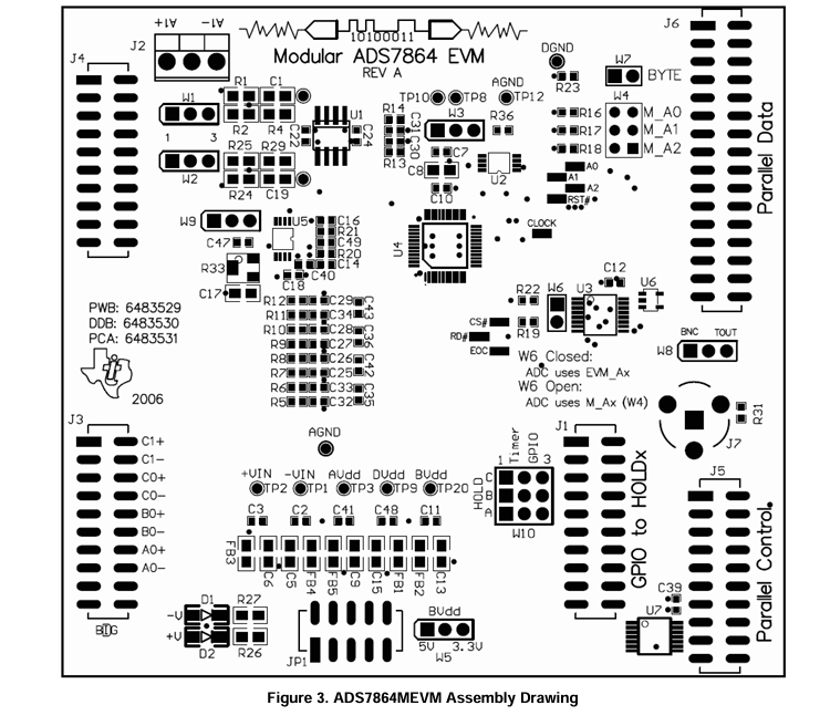
7.Assembly Drawing
- LP8557IEVM_TI(德州仪器)中文资料_英文资料_价格_PDF手册
- LAUNCHXL-F28027F TI(德州仪器)中文资料_英文资料_价格_PDF手册
- DLPDLCR160CPEVM DLP160CP TI(德州仪器)中文资料_英文资料_价格_PDF手册
- THS4631DDAEVM TI(德州仪器)中文资料_英文资料_价格_PDF手册
- DAC3482EVM TI(德州仪器)中文资料_英文资料_价格_PDF手册
- THS4302EVM TI(德州仪器)中文资料_英文资料_价格_PDF手册
- ADS7038Q1EVM-PDK_TI(德州仪器)中文资料_英文资料_价格_PDF手册
- LM3450AEV230V30/NOPB_TI(德州仪器)中文资料_英文资料_价格_PDF手册
- TPS72728DSEEVM-406_TI(德州仪器)中文资料_英文资料_价格_PDF手册
- WL1835MODCOM8A_TI(德州仪器)中文资料_英文资料_价格_PDF手册
- TAS5424BQ1DKDEVM_TI(德州仪器)中文资料_英文资料_价格_PDF手册
- ADS7042EVM-PDK_TI(德州仪器)中文资料_英文资料_价格_PDF手册
- TMDS570LS31HDK_TI(德州仪器)中文资料_英文资料_价格_PDF手册
- VCA8500BOARD_TI(德州仪器)中文资料_英文资料_价格_PDF手册
- DEM-SOT223LDO_TI(德州仪器)中文资料_英文资料_价格_PDF手册
 工商网监
工商网监