
TLV9061DPWEVM
适用于采用 0.8mm x 0.8mm (X2SON) 封装、超小型运算放大器的评估模块
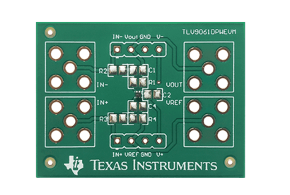
This user's guide contains support documentation for the TLV9061DPWevaluationmodule (EVM). Includedinthisdocument isadescriptionofhowtosetupandconfiguretheEVM,printedcircuitboard (PCB) layout,schematic,andbillofmaterials(BOM)fortheTLV9061DPWEVM.
1.Introduction
The TLV9061 is a high-performance, low cost, low power operational amplifier. For a full list of electrical
characteristics of the TLV9061, please refer to the TLV9061 product data sheet (SBOS839). This EVM is
developed to give users the ability to easily evaluate their design concepts using the TLV9061. The EVM
can be configured into three circuit configurations: difference amplifier, non-inverting amplifier and
inverting amplifier by populating different components on board.
2.TLV9061DPWEVM Kit Contents
Table 1 details the contents included in the TLV9061DPWEVM kit.

3
Circuit Configurations
2
By populating different components on the PCB, the TLV9061DPWEVM can be configured into three
different circuits:
• Difference amplifier
• Non-inverting amplifier
• Inverting amplifier
4 SchematicandPCBLayout
ThissectionprovidestheschematicandPCBlayoutof theTLV9061DPWEVM.Alsoincludedarethe
schematicsforthethreeTLV9061DPWEVMcircuitconfigurationoptions.
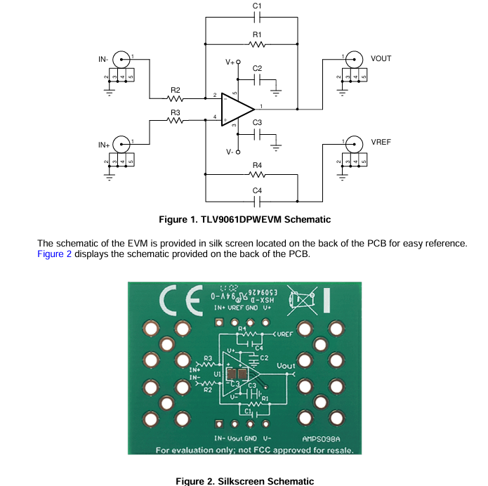
4.1 Schematic
Figure1displaysthecircuitschematicof theTLV9061DPWEVM.
4.2 Difference Amplifier
Figure 3 displays the schematic for the difference amplifier circuit configuration.
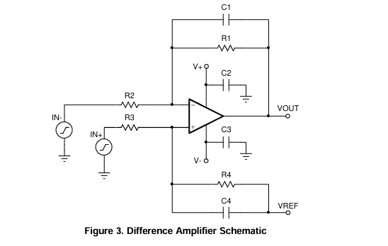
Equation 1 displays the transfer function of the difference amplifier circuit configuration.
If R1 = R4 and R2 = R3, Equation 1 can simplify to Equation 2.
Capacitors C1 and C4 provide the option to filter the output of the amplifier. Equation 3 calculates the
cutoff frequency, fc
, of the filter.
Where
• R1=R4,R2=R3,and C1 =C4
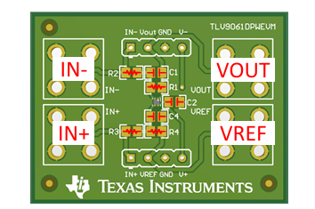
Figure 4 displays the TLV9061DPWEVM populated with the required components to be configured as a
difference amplifier.
4.3 Non-inverting Amplifier
Figure 5 displays the schematic for the non-inverting amplifier circuit configuration. To configure the EVM
in a non-inverting configuration short R3 using a 0-Ω resistor or solder bridge, leave R4 and C4
unpopulated, and ground the input connection IN–. The input signal is applied directly to the high
impedance non-inverting input terminal using the IN+ connection on the EVM.
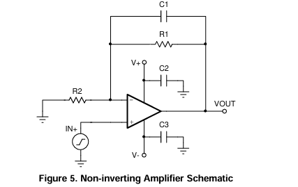
Equation 4 displays the DC transfer function of the non-inverting amplifier circuit configuration shown in
Figure 5.
(4)
Capacitor C1 provides the option to filter the output. The cutoff frequency, fc
, of the filter can be calculated
using Equation 5.
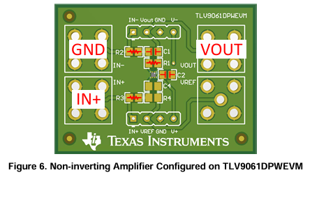
Figure 6 displays the TLV9061DPWEVM populated with the required components to be configured as a
non-inverting amplifier.
4.4 Inverting Amplifier
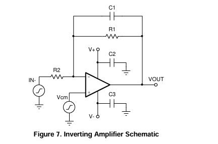
Figure 7 shows the schematic for the inverting amplifier circuit configuration. To configure the EVM in an
inverting configuration short R3 using a 0-Ω resistor or solder bridge, leave R4 and C4 unpopulated, and
apply the desired common mode voltage to the input connection, IN+. The input signal is applied using the
input connection IN–
4.4 PCBLayout
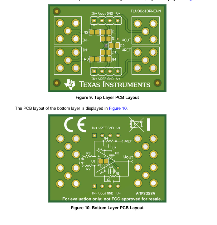
The TLV9061DPWEVM is a two layer board. The PCB layout of the top layer is displayed in Figure 9
- LP8557IEVM_TI(德州仪器)中文资料_英文资料_价格_PDF手册
- LAUNCHXL-F28027F TI(德州仪器)中文资料_英文资料_价格_PDF手册
- DLPDLCR160CPEVM DLP160CP TI(德州仪器)中文资料_英文资料_价格_PDF手册
- THS4631DDAEVM TI(德州仪器)中文资料_英文资料_价格_PDF手册
- DAC3482EVM TI(德州仪器)中文资料_英文资料_价格_PDF手册
- THS4302EVM TI(德州仪器)中文资料_英文资料_价格_PDF手册
- ADS7038Q1EVM-PDK_TI(德州仪器)中文资料_英文资料_价格_PDF手册
- LM3450AEV230V30/NOPB_TI(德州仪器)中文资料_英文资料_价格_PDF手册
- TPS72728DSEEVM-406_TI(德州仪器)中文资料_英文资料_价格_PDF手册
- WL1835MODCOM8A_TI(德州仪器)中文资料_英文资料_价格_PDF手册
- TAS5424BQ1DKDEVM_TI(德州仪器)中文资料_英文资料_价格_PDF手册
- ADS7042EVM-PDK_TI(德州仪器)中文资料_英文资料_价格_PDF手册
- TMDS570LS31HDK_TI(德州仪器)中文资料_英文资料_价格_PDF手册
- VCA8500BOARD_TI(德州仪器)中文资料_英文资料_价格_PDF手册
- DEM-SOT223LDO_TI(德州仪器)中文资料_英文资料_价格_PDF手册
 工商网监
工商网监