
LDO-PARAL-DESG-EVM
EV BRD TPS7B4253-Q1 TPS7B6750-Q1
Thisuser'sguidedescribesthecharacteristics,operation,anduseof theLDOParallelDesignevaluation module(EVM)andincludessetupinstructions,boardlayouts,schematics,andthebillofmaterials(BOM).
1 Introduction
TI'sLDOParallelDesignevaluationmodule(EVM)helpsdesignersevaluatetheoperationand performanceof theLDOparallelapplicationwiththeTPS7B6750-Q1andTPS7B4253-Q1inparallel.For moreinformationontheTPS7B6750-Q1andTPS7B4253-Q1devices,seethedatasheets(SLVSCB2 andSLVSCP3,respectively).
TheEVMcontainsthreelinearregulators(seeTable1).
2 Connector Descriptions, Setup, and Operation
This section describes the jumpers and connectors on the EVM as well and how to properly connect, set up, and use the LDO Parallel Design EVM.
2.1 Input and Output (I/O) Connector Descriptions
J1/VBAT connector– This connector connects the regulator IN pin to the input power supply through a diode.
J2/VOUT connector– This connector provides the output of the regulator to allow the user to attach a load to the EVM.
2.2 Bench Setup
The input voltage range for both the TPS7B6750-Q1 and TPS7B4253-Q1 is 4 V to 40 V. The EVM can support up to a 900-mA load current. Use the following steps to setup the test bench for the EVM: 1. Set the power supply for input (VBAT) to 12 V and set the current limit to 1 A. 2. Connect the power supply positive lead to the VIN (J1 VBAT) and the negative lead to GND (J1 GND). 3. Apply the load between OUT (J2 VOUT) and GND (J2 GND).
2.3 Operation
The LDO Parallel Design EVM powers up after the VIN voltage exceeds the UVLO rising threshold of both the TPS7B6750-Q1 and TPS7B4253-Q1.
3 Board Layout
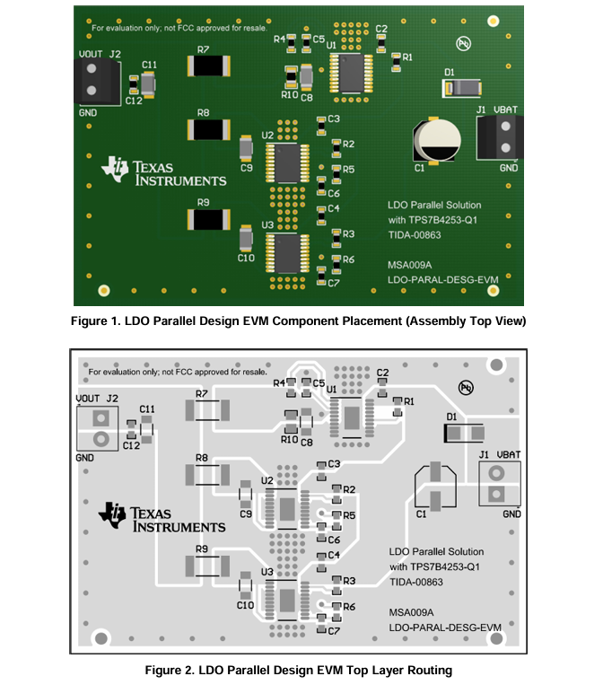
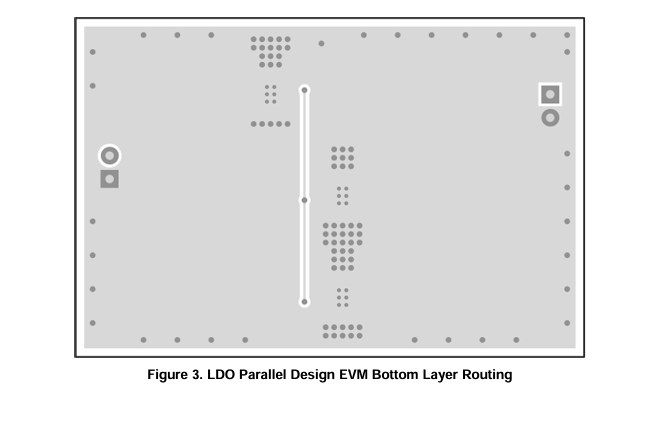
The PCB offers footprints for the LDO Parallel Design EVM as shown in Figure 1, Figure 2, and Figure 3.
4 Schematic and Bill of Materials
4.1 Schematic
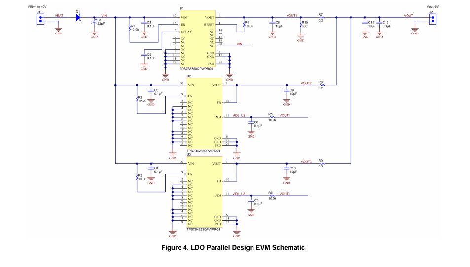
Figure 4 illustrates the EVM schematic.
- TLA2024EVM-PDK_TI(德州仪器)中文资料_英文资料_价格_PDF手册
- INA229_239EVM_TI(德州仪器)中文资料_英文资料_价格_PDF手册
- DAC8832EVM-PDK _TI(德州仪器)中文资料_英文资料_价格_PDF手册
- LP8557IEVM_TI(德州仪器)中文资料_英文资料_价格_PDF手册
- LAUNCHXL-F28027F TI(德州仪器)中文资料_英文资料_价格_PDF手册
- DLPDLCR160CPEVM DLP160CP TI(德州仪器)中文资料_英文资料_价格_PDF手册
- THS4631DDAEVM TI(德州仪器)中文资料_英文资料_价格_PDF手册
- DAC3482EVM TI(德州仪器)中文资料_英文资料_价格_PDF手册
- THS4302EVM TI(德州仪器)中文资料_英文资料_价格_PDF手册
- ADS7038Q1EVM-PDK_TI(德州仪器)中文资料_英文资料_价格_PDF手册
- LM3450AEV230V30/NOPB_TI(德州仪器)中文资料_英文资料_价格_PDF手册
- TPS72728DSEEVM-406_TI(德州仪器)中文资料_英文资料_价格_PDF手册
- WL1835MODCOM8A_TI(德州仪器)中文资料_英文资料_价格_PDF手册
- TAS5424BQ1DKDEVM_TI(德州仪器)中文资料_英文资料_价格_PDF手册
- ADS7042EVM-PDK_TI(德州仪器)中文资料_英文资料_价格_PDF手册
 工商网监
工商网监