
THS4552RTWEVM
TheTHS4552RTWEVMisanevaluationmodule for thedual THS4552amplifier in theRTW(24-pin VQFN)package.Thisevaluationmodule isdesignedtoquicklyandeasilydemonstratethefunctionality andversatilityof theamplifier.TheEVMisreadytoconnect topower,signalsource,andtest instruments through theuseof onboardconnectors.TheEVMcomesconfigured foreasyconnectionwithcommon 50-Ω laboratoryequipment on its inputsandoutputs. Theamplifier is configured for single-endedor differential inputwithgainof1V/Vtodifferential outputat thedevicepins,which isconvertedtosingle endedviaa transformer to theoutput.Both thechannelscanbeeasilyconfigured for other functions, gains,andsingle-orsplit-supplyoperation.
TheTHS4552RTWEVMhasanonboard load for theamplifier of 1kΩonbothchannels. Theoutput transformerandresistornetworkconvertsthistoa50-Ωsingle-endedoutput.
1 Features
This EVM supports the following features:
• Configured for split-supply operation and easily modified for single supply
• Default gain of 1 configuration can easily be reconfigured for other gains
• Designed for easy connection to standard 50-Ω input and output impedance test equipment
• Inputs and outputs include SMA connectors
2 EVM Specifications
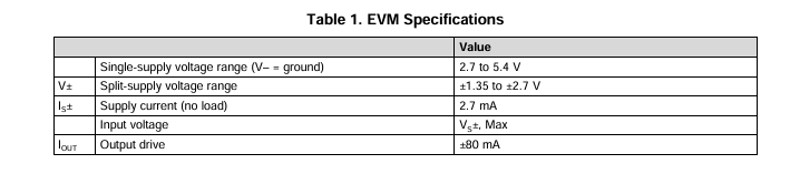
Table 1 lists the EVM specifications:
3 Power Connections
The THS4552RTWEVM is equipped with test point connectors for easy connection of power. The positive supply input is red and is labeled V+. The negative supply input is yellow and is labeled V–. The Ground is black and is labeled GND.
3.1 Split-Supply Operation
To operate as split supply, apply the positive supply voltage to V+, negative supply voltage to V– , and the ground reference from supply to GND.
3.2 Single-Supply Operation
To operate as single supply, connect both the V– connector and the GND connector to ground, and apply the positive supply voltage to V+. Inputs and outputs must be biased per datasheet specifications for proper operation. The THS4552 outputs common-mode voltage defaults to mid supply if the Vcm1 and Vcm2 connector is left floating.
4 Input and Output Connections
The THS4552RTWEVM is equipped with SMA connectors for easy connection of signal generators and analysis equipment. As shipped, the EVM is configured for a gain of 1, split supply, single-ended or differential input and single-ended output with 50-Ω termination on both the channels. For best results, signals must be routed to and from the EVM with cables having 50-Ω characteristic impedance. Either IN1+ (J1) or IN1– (J2) can be used for single-ended input on one channel and IN2+ (J3) or IN2– (J4) can be used for single-ended input on the other channel. The unused connector should be terminated with a 50-Ω resistive SMA load. If no SMA load is available, the spaces marked C1, C2, C17, or C18 can be loaded with a 0-Ω resistor to terminate the unused input. Use both IN1+ (J1) and IN1– (J2) for differential input on one channel and both IN2+ (J3) and IN2– (J4) for differential input on the other channel. OUT1+ (J12) is the output connector for single-ended output signal for one channel and OUT2+ (J14) is the output connector for single-ended output signal for the other channel. The amplifier converts the single-ended or differential input to a differential signal at its output pins. A resistor network and transformer on the output of the amplifier convert the differential output signal to single-ended, and provides a 1-kΩ load to the amplifier when terminated in 50 Ω. A 50-Ω line-impedance match at OUT1+ and OUT2+ should be preserved. This results in an output measurement loss, and the overall gain is approximately–30 dB. See the THS4552 datasheet applications section (SBOS831), schematics, and layouts for more detail and how to reconfigure the EVM.
4.1 VOCM Input Connections
The Vcm1 (J7) and Vcm2 (J6) inputs are optional and the SMA connectors are not loaded in default configuration. These inputs set the common mode of the output pins of both the channels independently. The THS4552 will automatically self-bias the output common-mode voltages to the mid-supply voltage if the VOCM1 or VOCM2 pins are not connected. This is the optimal voltage for maximum output swing and best linearity.
The valid range of the VOCM1 and VOCM2 is 0.55 V above the negative supply to 1.5 V below the positive supply. For example, on a ±2.5-V split supply, the VOCM1 and VOCM2 pin can be set anywhere from–1.95 V to 1.0 V. With a single 5-V supply the valid range would be 0.55 V to 3.5 V. Remember, the outputs of the THS4552 can swing from rail to rail; however, the maximum output swing available is reduced when the output common mode is set to a voltage other than mid supply.
If providing 50-Ω termination for the Vcm1 or Vcm2 input signal source is desired, C6 or C20 can be
replaced with a 0-Ω resistor, respectively. The board is shipped with C6 and C20 populated with 0.22 µF
and output common mode voltages of both channels are set to mid-supply voltage with C6 and C20
populated.
4.2 PD Input Connections
The PD1 (J5) and PD2 (J10) jumpers allow both THS4552 channels to be disabled independently. SMA connectors can also be loaded at J8 and J9 and a signal for the power down function can be applied for high-speed testing. Normally the J5 and J10 jumpers are used to enable or disable (power down) the corresponding channels of the dual-channel amplifier. When the jumpers are open, the amplifier is not powered down, so it is enabled. When the shorting block is connected and J5 or J10 is closed, the amplifier channel corresponding to the jumper is powered down.
For high-speed testing, the C4 and C19 can be replaced with 0 Ω to terminate the PD1 and PD2 SMA
inputs, respectively. The shorting block should be removed from J5 and J10 during high-speed testing.
Because 0 Ω at C4 or C19 terminates to the ground and not to the supplies, the state of the amplifier will
be undefined when the signal source is disconnected. For this reason, 0 Ω at C4 or C19 should only be
used when driving the SMA connector with a high-speed, controlled-impedance source.
5 THS4552RTWEVMSchematic,Layout,andBillofMaterials
5.1 Schematics
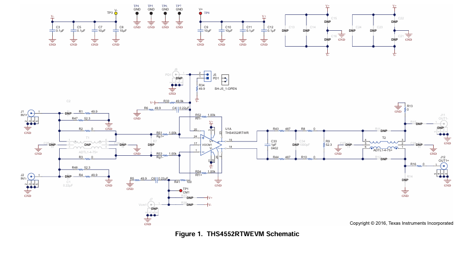
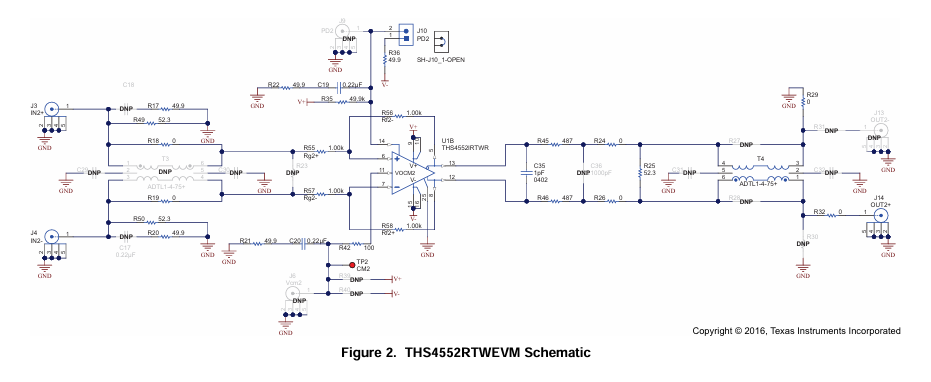
Figure1andFigure2illustratetheEVMschematics.
5.2 THS4552RTWEVM Layers
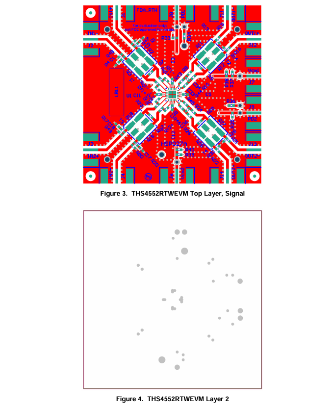
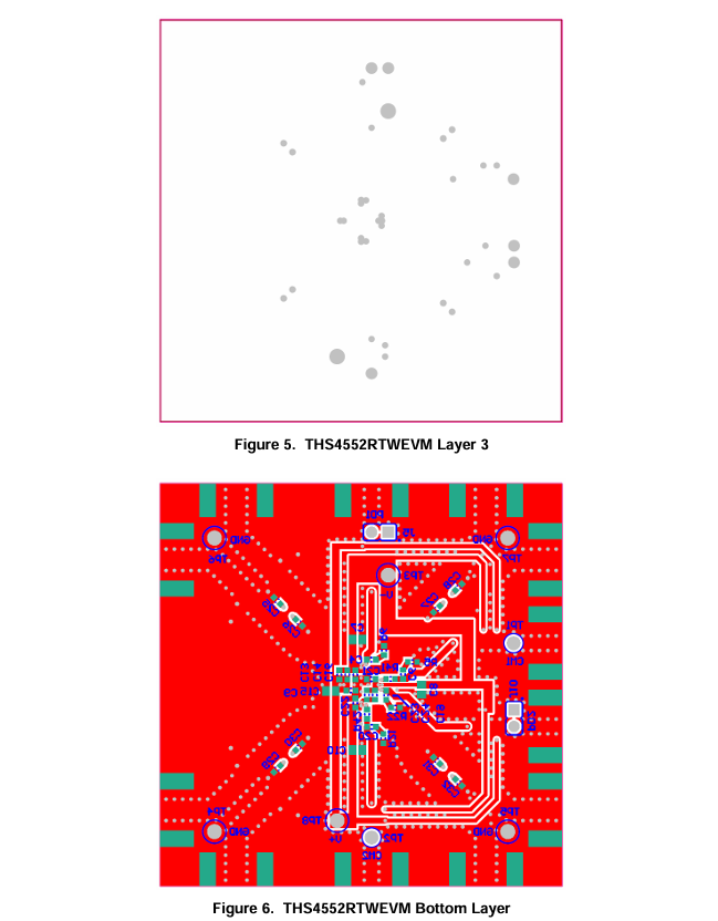
Figure 3 through Figure 6 show the THS4552RTWEVM layers.
- TLA2024EVM-PDK_TI(德州仪器)中文资料_英文资料_价格_PDF手册
- INA229_239EVM_TI(德州仪器)中文资料_英文资料_价格_PDF手册
- DAC8832EVM-PDK _TI(德州仪器)中文资料_英文资料_价格_PDF手册
- LP8557IEVM_TI(德州仪器)中文资料_英文资料_价格_PDF手册
- LAUNCHXL-F28027F TI(德州仪器)中文资料_英文资料_价格_PDF手册
- DLPDLCR160CPEVM DLP160CP TI(德州仪器)中文资料_英文资料_价格_PDF手册
- THS4631DDAEVM TI(德州仪器)中文资料_英文资料_价格_PDF手册
- DAC3482EVM TI(德州仪器)中文资料_英文资料_价格_PDF手册
- THS4302EVM TI(德州仪器)中文资料_英文资料_价格_PDF手册
- ADS7038Q1EVM-PDK_TI(德州仪器)中文资料_英文资料_价格_PDF手册
- LM3450AEV230V30/NOPB_TI(德州仪器)中文资料_英文资料_价格_PDF手册
- TPS72728DSEEVM-406_TI(德州仪器)中文资料_英文资料_价格_PDF手册
- WL1835MODCOM8A_TI(德州仪器)中文资料_英文资料_价格_PDF手册
- TAS5424BQ1DKDEVM_TI(德州仪器)中文资料_英文资料_价格_PDF手册
- ADS7042EVM-PDK_TI(德州仪器)中文资料_英文资料_价格_PDF手册
 工商网监
工商网监