
LMH6517EVAL-R1/NOPB
1 General Description
The LMH6517EVAL-R1 evaluation board is designed to aid in the characterization of Texas Instruments'High Speed LMH6517 Digital Controlled Variable Gain Amplifier (DVGA).
The evaluation board is used as a guide for high frequency layout and as a tool to aid in device testing and characterization.
2 Basic Operation
The LMH6517 DVGA has differential inputs and differential outputs. To aid evaluation with 50Ω, single ended test equipment the LMH6517EVAL-R1 evaluation board is shipped with transformers on both the input and output signal paths. The single ended signal path uses the IN+ and OUT+ marked connectors. The IN− and OUT− signal paths are grounded and the SMA connectors are not installed.
The input and output pins of the LMH6517 will self bias to approximately mid supply (2.5V). The LMH6517EVAL-R1 board has been designed with AC coupling on both input and output signal paths to protect test equipment and to ensure proper operation of the LMH6517 DVGA. Any modifications to the board should preserve the operating points of the DVGA and protect sensitive test equipment.
Transformers T1– T4 can provide both impedance matching as well as single ended to differential conversion. The board is shipped with 2:1 turns ratio (4:1 impedance ratio) transformers that will match 50Ω equipment with the 200Ω input impedance of the LMH6517 DVGA . Do not connect the transformer secondary winding directly to ground since this will short the DVGA input voltage to ground.
For differential operation the board must be modified by hand. The copper on the grounded input must be cut as illustrated in Figure 7. and additional SMA connectors need to be soldered to the board to complete the IN- and OUT- signal paths. The LMH6517EVAL-R1 Evaluation board is 0.63” thick and uses edge mounted SMA connectors. The board is built with Emerson part #142–0701–806 end launch, nickel plated SMA connectors.
The LMH6517EVAL-R1 evaluation board comes built with 1:1 balun transformers and 10 Ohm series output resistors (R42, R43, R44 and R45). A 4.7pF load capacitor is placed between the resistors and the transformer (C14 and C15). The 10 Ohm resisters and 4.7pF capacitor form a snubber circuit that reduces high frequency peaking and enhances stability. The combination of the snubber circuit and the 1:1 balun gives very good power gain and very good OIP3 performance when driving 50Ω test equipment. The output impedance of the LMH6517 amplifier is very low (<2Ω @ 50MHz). Many load conditions can be achieved by changing out the components on the evaluation board. Not all load conditions will require a snubber circuit, but it should be included in the final circuit design unless sufficient testing has shown it to be unnecessary.
The capacitors C5, C7, C8 and C9 isolate the output transformer from the output SMA connectors and are not required if the transformer provides DC blocking. The spaces marked C34, C35, C36 and C37 are left empty by the factory. These positions are included to provide the flexibility to add extra components. Capacitors can be added to create a low pass filter. Resistors could be placed in these locations to create different load conditions for the amplifier.
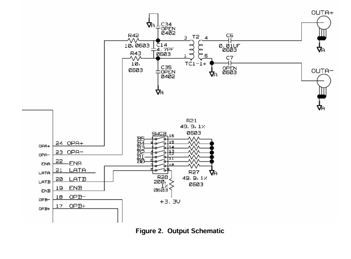
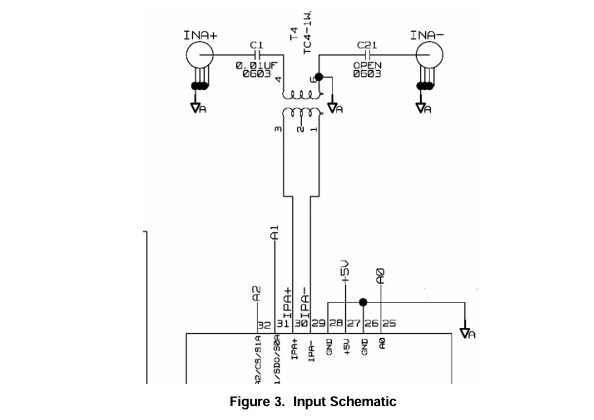
The board was designed to be very flexible for many different configurations. Zoomed in portions of the input and output schematics are shown above in Figure 2 and Figure 3. The evaluation board, as shipped, has been optimized for ease of use with single ended 50 Ohm test equipment. This configuration may not emulate the most common application circuits. The signal path schematic is shown in Figure 8 and the full schematic in . PDF format is available upon request.
3 Using with Different Sources or Loads
The LMH6517EVAL-R1 evaluation board supports differential operation on both inputs and outputs. However they will require additional components and some board rework. For driving the evaluation board from a differential source, symmetrical signal paths are provided. Both input and output paths support fully differential test equipment.
To drive the LMH6517EVAL-R1 evaluation board from a differential source, the transformers T3 and T4 must be removed. The diagrams in Figure 6 and Figure 7 show the required connections for differential inputs. DC coupled operation is possible using differential signals. For DC coupled operation, make sure that the test equipment can provide the 2.5 V offset voltage required.
For differential output signals remove transformers T1 and T2. Wire jumpers or zero Ohm resistors must be added to complete the signal path across the transformer pads similar to the changes required for differential inputs
4 Other Board Configurations
For other applications or experiments there are many options for changing the output circuit to simulate different circuit conditions. One option is to use a 2:1 transformer to simulate high impedance loads. In this case one would use 100 Ohm resistors for R42, R43, R44 and R45. This would present a load of 200 Ohms to the amplifier output. Many common filter circuits have 200 Ohm input impedance. Other combinations can also be used to simulate different load conditions. With a high impedance load the capacitors C14 and C15 should be decreased to 1pF to avoid losing bandwidth.
Near the power connector are a number of 0.1” pitch headers. The header labeled J1 provides off board access to the LMH6517 digital control pins. The J1 pins and functions are described below. The jack labeled J10 is normally loaded with a shorting jumper, it provides power to a 3.3V power supply used to provide 3.3V logic signals to the digital pins. The jack labeled J11 is also loaded with a shorting block and it provides the 5V power to the LMH6517. By removing the short on this jack and replacing it with an ammeter the current drawn by the DVGA can be measured. The jack labeled J12 is a ground connector and is normally left empty.
Near the power connector are a number of 0.1” pitch headers. The header labeled J1 provides off board access to the LMH6517 digital control pins. The J1 pins and functions are described below. The jack labeled J10 is normally loaded with a shorting jumper, it provides power to a 3.3V power supply used to provide 3.3V logic signals to the digital pins. The jack labeled J11 is also loaded with a shorting block and it provides the 5V power to the LMH6517. By removing the short on this jack and replacing it with an ammeter the current drawn by the DVGA can be measured. The jack labeled J12 is a ground connector and is normally left empty.
5 Additional Design Tools
The RD-179: High-IF Sub-sampling Receiver Subsystem board (SP16160CH1RB) is also available. This reference design includes the ADC16DV160 ADC, the LMH6517 DVGA, and the LMK04031B precision clock conditioner. Power regulation, filters and controlled impedance board layout are all provided in this reference design.
- TLA2024EVM-PDK_TI(德州仪器)中文资料_英文资料_价格_PDF手册
- INA229_239EVM_TI(德州仪器)中文资料_英文资料_价格_PDF手册
- DAC8832EVM-PDK _TI(德州仪器)中文资料_英文资料_价格_PDF手册
- LP8557IEVM_TI(德州仪器)中文资料_英文资料_价格_PDF手册
- LAUNCHXL-F28027F TI(德州仪器)中文资料_英文资料_价格_PDF手册
- DLPDLCR160CPEVM DLP160CP TI(德州仪器)中文资料_英文资料_价格_PDF手册
- THS4631DDAEVM TI(德州仪器)中文资料_英文资料_价格_PDF手册
- DAC3482EVM TI(德州仪器)中文资料_英文资料_价格_PDF手册
- THS4302EVM TI(德州仪器)中文资料_英文资料_价格_PDF手册
- ADS7038Q1EVM-PDK_TI(德州仪器)中文资料_英文资料_价格_PDF手册
- LM3450AEV230V30/NOPB_TI(德州仪器)中文资料_英文资料_价格_PDF手册
- TPS72728DSEEVM-406_TI(德州仪器)中文资料_英文资料_价格_PDF手册
- WL1835MODCOM8A_TI(德州仪器)中文资料_英文资料_价格_PDF手册
- TAS5424BQ1DKDEVM_TI(德州仪器)中文资料_英文资料_价格_PDF手册
- ADS7042EVM-PDK_TI(德州仪器)中文资料_英文资料_价格_PDF手册
 工商网监
工商网监