
TPS7A7200EVM-718
Thisuser’sguidedescribesthefunctionaloperationof theTPS7A7200EVM-718evaluationmodule(EVM) foruseasareferencedesignandasgeneralengineeringdemonstrationfortheTPS7A7100,TPS7A7200, andTPS7A7300 low-dropout (LDO) linear regulators.EVMscontaining theseother regulator integrated circuits of the same family, andusing the sameprinted-circuit boardand circuitry areavailableand orderable. Included inthisuser’sguidearesetup instructions,aschematicdiagram, layoutandthermal guidelines,abillofmaterials,andtestresults.
1 Introduction
EachofTexasInstrumentsEVMs, theTPS7A7100EVM-718, theTPS7A7200EVM-718,andthe TPS7A7300EVM-718, isdesignedwithidenticalcircuitry,excludingtheLDOregulator itself, tohelp engineersevaluatetheoperationandperformanceof theTPS7A7x00linearregulatorforpossibleusein theirowncircuitapplication.Notablefeaturesof theseLDOregulatorsincludethermalandcurrent-limit shutdownprotection,aPowerGoodfunction,pin-selectableoutputvoltage, lowdropout,andwideband performance.TheEVMcontainsasinglelinearregulator ina5-mmx5-mm,QFN(RGW), thermally enhanced,PowerPad™package.Thisregulator, includingexternalcomponents, iscapableofdelivering upto3A(dependingontheLDOregulator)toadynamicloadacrossthefull recommendedinputand outputvoltagerangeof theLDOregulator.Amultipinheaderwithjumpersisprovidedtoenableeasy manualselectionof theoutputvoltage.
2 Setup
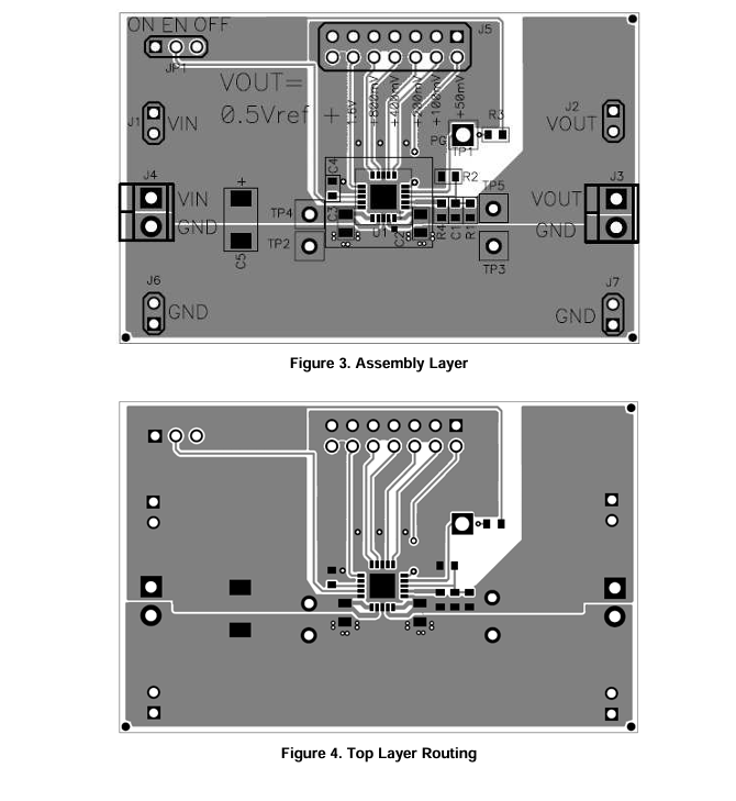
This section describes the connectors and headers on the EVM as well as how to properly connect, set up and use the TPS7A7x00EVM-718. See the Assembly Layer diagram, Figure 4, for the location and orientation of referenced components.
2.1 Input/Output Connector-Headers and Jumper Descriptions
• J1-VIN– Positive (+) input power supply voltage test and measurement header.
• J2–VOUT–Output voltage test and measurement header.
• J3(pin 1)– VOUT– Regulator output to a high-current load (up to 6 A).
• J3(pin 2)– GND– Ground return from the load (up to 6 A)
• J4(pin 1)– VIN– Positive (+) input power supply connector
• J4(pin 2)– GND– Negative (–) input power supply return connector. See preceding J4–VIN (pin 1) note.
• J5-Header for setting the output voltage. Output Voltage Set: The output voltage is set by jumpering J5 header pins, each assigned to a given voltage level, to ground where VOUT = Vref + (sum of jumper-voltages). J5 header pins are numbered sequentially, odd pins (1,3,5, …, 13) ascending leftward of pin 1 on the top row. All odd pins are connected to ground. Each even pin is numbered right to left sequentially (2,4,6,…,14) on the bottom row; and each even pin is assigned a unique voltage level. See the pin-to-pin output voltage assignments in the following table.
• J6–GND–Ground header for test and measurement of VIN.
• J7–GND–Ground header for test and measurement of VOUT.
• JP1–EN–Enable (Disable) header. Enable the LDO output by shorting EN (pin 2) to ON (pin 1).
Disable the LDO output by shorting EN (pin 2 ) to OFF (pin 3).
• TP1–Power Good (PG) test point.
• TP4–VINtest point for most accurate measurement of the input voltage characteristics.
• TP2–Ground test point to be used with TP4.
• TP5–VOUTtest point for most accurate measurement of the output voltage.
• TP3–Ground test point to be used with TP5.
2.2 Soldering Guidelines
Any solder rework to modify the EVM for the purpose of repair or other application reasons must be performed using a hot-air system to avoid damaging the integrated circuit IC especially.
2.3 Initial Setup and Equipment Interconnect
• VOUTSelect. Program the desired output voltage per instruction 2.1, bullet J5. Use the shorting jumpers provided with the EVM to jumper the header pins. Note that the EVM is preset for VOUT equal to 1.8 V. The jumper across J5 pins 13 to 14 is no-connect and unused.
• Disable the EVM. Add a shorting jumper to JP1 from EN (pin 2) to OFF (pin3)
• Input Power Supply connection. Before connecting the input power supply to the EVM, verify that its output voltage is set to the desired supply voltage (less than 6.5 V) and that its current limit is set to approximately 4 A. Now turn off the power supply. Connect the positive voltage lead (+) from input power supply to VIN (J4, pin 1) of the EVM. Connect the ground lead (–) from the input power supply to GND (J4, pin 2). Note that for the recommended best thermal and ac performance, ensure that the input voltage at TP4 is 0.5 V to 1 V above VOUT.
• Connect a 0-A to 2-A load between VOUT (J3, pin 1) and GND (J3, pin 2).
3 Operation
• Turn on the input power supply. Verify that the output voltage, VOUT, is near 0 V.
• Enable the output by reconnecting the jumper on JP1 to short the EN (pin 2) to the ON (pin 1).
• Vary the load current and VIN voltage as necessary for test purposes. Note that power dissipation (Pdisp ) across the TPS7A7X00 itself depends on the VIN-to-VOUT voltage drop and the output load current, ILoad (Pdisp = (VIN– VOUT)×ILoad ). If the power dissipation is high, then the customer may see the output voltage transitioning on-off-on due to the shutdown effect of the thermal-limit shutdown circuit
4 Test Results
This section provides typical performance waveforms for the TPS7A4001EVM-709 characteristic of this EVM design.
4.1 Turnon Characteristic
Figure 1 shows the VOUT ramp-up waveform at turnon (ENable) as well as the input surge current into the IN pin of the LDO itself when the LDO starts up into a fully loaded output.
5 Thermal Guidelines and Layout Recommendation
Thermal management is a key consideration in the design of any dc-dc converter but is especially important for an LDO regulator when the power dissipation is high. Use Equation 1 to approximate the worst-case junction temperature for the application:TJ = TA + Pd x θJA
where TJ is the junction temperature (°C), TA is the ambient temperature (°C), Pd is the power dissipation in the device (W), and θJA is the thermal resistance from junction to ambient (°C/W). The maximum silicon junction temperature must not be allowed to exceed 125°C for reliable operation. The layout design must use copper trace and plane areas smartly, as thermal sinks, so as to not allow TJ to exceed the absolute maximum rating under all load, voltage, and temperature conditions for a given application.
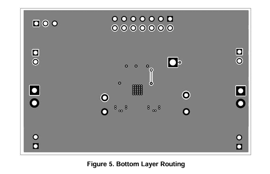
The designer must carefully consider the thermal design of the printed-circuit board (PCB) for optimal performance over temperature. For this EVM, Figure 6 shows that the RGW package footprint employs a square thermal pad, centered under the device, for conducting heat to the copper-spreading layers of the PCB. The thermal pad is soldered directly to a pad on the PCB containing a 5x5 pattern of 10-mil vias for conducting heat to the bottom-side ground plane copper. Approximately 4 in2 of 2-oz copper is used on the bottom side of the EVM for dissipating heat generated by the LDO regulator.
Table 1 is based on thermal resistance information from the Thermal Information Table of the TPS7A7x00 data sheet for comparison with the approximate thermal resistance, θJA , calculated for this EVM layout to show the variation in junction-ambient thermal resistances for varying copper areas. The High-K thermal resistance, θJA , is determined using a standard JEDEC High-K (2s2p) board having dimensions of 3-inch x 3-inch with two 1-oz internal power and ground planes and one 2-oz copper bottom plane for spreading/sinking heat from the IC component.
The thermal resistance for the TPS7A7A00EVM-718 is the measured value for this particular layout scheme. The maximum power dissipation is proportional to the volume of copper volume connected to the package.
6 Board Layouts
7 Schematic and Bill of Materials
7.1 Schematic
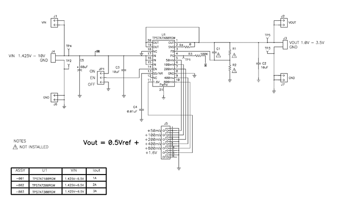
7.2 Bill of Materials
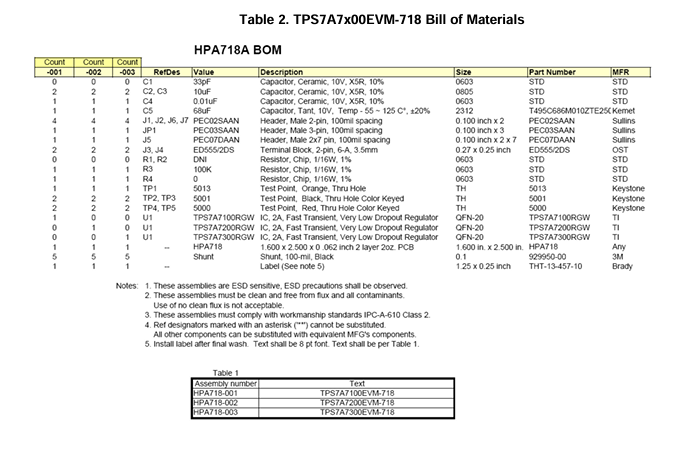
- TLA2024EVM-PDK_TI(德州仪器)中文资料_英文资料_价格_PDF手册
- INA229_239EVM_TI(德州仪器)中文资料_英文资料_价格_PDF手册
- DAC8832EVM-PDK _TI(德州仪器)中文资料_英文资料_价格_PDF手册
- LP8557IEVM_TI(德州仪器)中文资料_英文资料_价格_PDF手册
- LAUNCHXL-F28027F TI(德州仪器)中文资料_英文资料_价格_PDF手册
- DLPDLCR160CPEVM DLP160CP TI(德州仪器)中文资料_英文资料_价格_PDF手册
- THS4631DDAEVM TI(德州仪器)中文资料_英文资料_价格_PDF手册
- DAC3482EVM TI(德州仪器)中文资料_英文资料_价格_PDF手册
- THS4302EVM TI(德州仪器)中文资料_英文资料_价格_PDF手册
- ADS7038Q1EVM-PDK_TI(德州仪器)中文资料_英文资料_价格_PDF手册
- LM3450AEV230V30/NOPB_TI(德州仪器)中文资料_英文资料_价格_PDF手册
- TPS72728DSEEVM-406_TI(德州仪器)中文资料_英文资料_价格_PDF手册
- WL1835MODCOM8A_TI(德州仪器)中文资料_英文资料_价格_PDF手册
- TAS5424BQ1DKDEVM_TI(德州仪器)中文资料_英文资料_价格_PDF手册
- ADS7042EVM-PDK_TI(德州仪器)中文资料_英文资料_价格_PDF手册
 工商网监
工商网监