
ADS5402EVM
ADS5402EVM 双通道、高达 800MSPS 的 ADS5402 评估模块
Thisuser'sguidedescribes theoperationof theTexas InstrumentsADS540xorADS54T0xevaluation module(EVM).TheEVMprovidesaplatformforevaluatingtheADS540xorADS54T0x,atwo-channel, 12-bitADCoperatingatsamplingratesofupto800MSPSwiththedigitaldataoutputontwo12-bitLVDS parallelbussesonaSamtecconnector.
ThisEVMisideallysuitedformatingwiththeTSW1400orTSW1405CaptureCardforperformingadata capture intoacapturebuffer, uploading thesampledata toaPC, performingaFastFourierTransform (FFT), and reportingon signal-to-noise ratio (SNR), spurious-freedynamic range (SFDR), andother performancemetrics.
1 Introduction
1.1 EVM Block Diagram
Figure 1 shows a simplified block diagram of the default configuration of the EVM. Each analog input is supplied to the EVM through a single-ended SMA connection, then transformer coupled to turn the single ended signal into a balanced differential signal, and then input to the ADS540x. A dual transformer input circuit is used for better phase and amplitude balance of the input signal than would typically be produced by a single transformer input circuit.
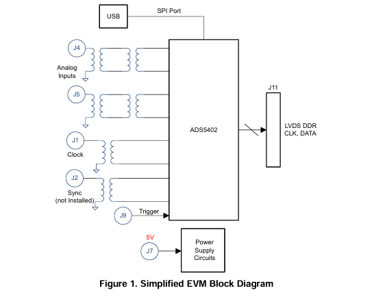
The clock input is supplied by way of a single-ended signal to an SMA connector and transformer coupled to produce a differential clock signal for the ADS540x
Power to the EVM is supplied using a single 5-V connection by way of banana jacks. All necessary voltages for the ADS540x are derived from the 5-V input connection
For the ADS54T0x EVM, a trigger signal may be input to the trigger SMA connector to trigger the burst of high resolution sample data from the ADC. This trigger signal may be sourced by the TSW1400 Capture Card
1.2 EVM Power Supply
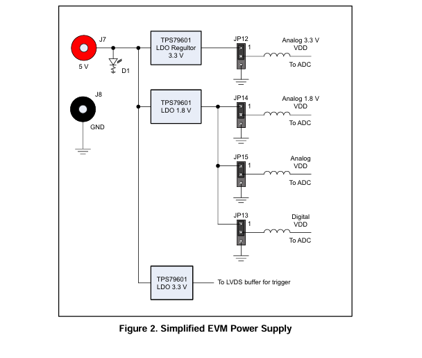
Figure 2 illustrates the power supply options available on the EVM. Jumpers are used to choose the power supply options, with the default jumper positions indicated by the darker portion of the jumper that represents the presence of the jumper.
low dropout (LDO) regulators are used to generate the 1.8 V for the analog and digital supplies for the ADS540x, the 3.3 V for the 3.3-V analog supply of the ADS540x, and the 3.3-V supply needed for an LVDS buffer to buffer the optional trigger signal into the ADS540x.
1.3 EVMJumpersandSwitches
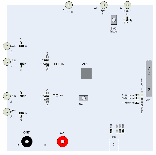
Thereareanumberof jumpersontheEVMforselectingoperationalmodesof theADC,powersupply options,andSPIportoptions.Manyof thejumperselectionsthat involveDCinputsorstaticcontrol signalsarebywayofpush-onsquarepost jumpers.Figure3illustratesthepositionof thejumpersrelative tothemorerecognizablefeaturesof theEVMsuchasthebananajacksorSMAinputs.Jumperselections that involvehigh-speedswitchingsignalsareimplementedbywayofsurfacemount0-Ωjumperresistors, andthesearerepresentedinFigure4. Inbothfigures,defaultpositionsof thejumpersastheEVMis normallyshippedareindicated.Notethatsomeof thejumpersare,bydefault, leftopencircuit.The surface-mount jumperresistorsrequiresolderingtochangefromdefault toanyotherdesired configuration.
Thefunctionsof theconnectors,LEDsandpushbuttonswitchesaredescribedbytheir labelsinFigure2. Thepresenceof the5-VsupplyvoltagestotheEVMisindicatedbyLEDD1lighting.
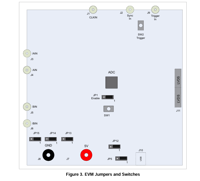
TherearetwopushbuttonswitchesontheEVM.PushbuttonswitchSW1isusedtoassertaresetsignal totheADS540x.TheADS540xrequiresaresetbeforeit isconfiguredforuse,but it isnotnecessaryto useSW1.TheADS540xSPIGUImaybeusedtotoggletheresetregisterbit intheADS540xregister map.Thetriggersignal totheADS54T0xmaybesourcedbytheSMAconnectorJ9, theSamtecconnectorJ11, orthepushbuttonSW2dependingonthepositionof thesurfacemount jumperSJP1.
1.4 EVM Solder Options
- TLA2024EVM-PDK_TI(德州仪器)中文资料_英文资料_价格_PDF手册
- INA229_239EVM_TI(德州仪器)中文资料_英文资料_价格_PDF手册
- DAC8832EVM-PDK _TI(德州仪器)中文资料_英文资料_价格_PDF手册
- LP8557IEVM_TI(德州仪器)中文资料_英文资料_价格_PDF手册
- LAUNCHXL-F28027F TI(德州仪器)中文资料_英文资料_价格_PDF手册
- DLPDLCR160CPEVM DLP160CP TI(德州仪器)中文资料_英文资料_价格_PDF手册
- THS4631DDAEVM TI(德州仪器)中文资料_英文资料_价格_PDF手册
- DAC3482EVM TI(德州仪器)中文资料_英文资料_价格_PDF手册
- THS4302EVM TI(德州仪器)中文资料_英文资料_价格_PDF手册
- ADS7038Q1EVM-PDK_TI(德州仪器)中文资料_英文资料_价格_PDF手册
- LM3450AEV230V30/NOPB_TI(德州仪器)中文资料_英文资料_价格_PDF手册
- TPS72728DSEEVM-406_TI(德州仪器)中文资料_英文资料_价格_PDF手册
- WL1835MODCOM8A_TI(德州仪器)中文资料_英文资料_价格_PDF手册
- TAS5424BQ1DKDEVM_TI(德州仪器)中文资料_英文资料_价格_PDF手册
- ADS7042EVM-PDK_TI(德州仪器)中文资料_英文资料_价格_PDF手册
 工商网监
工商网监