TPS61500EVM-369
This user’s guide describes the characteristics, operation, and use of the TPS61500EVM-369 evaluation module (EVM). This EVM contains the Texas Instruments TPS61500 boost converter, configured with external components to regulate current through a string of WLEDs. This user’s guide includes EVM specifications, recommended test setup, test results, bill of materials, and a schematic diagram.
1 Introduction
The Texas Instruments TPS61500EVM-369 evaluation module contains a TPS61500 boost converter IC, supporting active and passive components, and 5 white light-emitting diodes (WLEDs) in series. The goal of this EVM is to facilitate evaluation of the TPS61500 in a typical WLED application.
1.1 Performance Specification Summary
able 1 provides a summary of the TPS61500EVM-369 performance specifications. All specifications are given for an ambient temperature of 25°C.

1.2 Modifications
To aid user customization of the EVM, the board was designed with devices having 0603 or larger footprints. Actual implementations may occupy less space.
2 TPS61500EVM-369 Setup
2.1 Input/Output Connections
The connection points and jumper positions are described in the following paragraphs.
2.1.1 J1 – VIN
This header is the positive connection for the input power supply. The leads to the input supply should be twisted and kept as short as possible. The input voltage should remain within the limits specified in Table 1.
2.1.2 J2 – GND
This header is the return connection to the input power supply
2.1.3 J3 – VOUT
This header is the positive output of the device
2.1.4 J4 – GND
This header is the return connection for the load.
2.1.5 J5 – FB
This header is connected to the FB pin of the TPS61500, which is regulated to 0.2 V typical. This point is also connected to the anode of the last WLED in the on-board WLED string.
2.1.6 JP1 – Enable
This jumper connects the enable pin of the TPS61500 to either VIN (enabling the TPS61500) or GND (disabling the TPS61500). The jumper must be installed in one position only. Do not leave JP1 open.
2.1.7 JP2 – Open WLED
Installing this jumper connects the on-board WLED string to the output of the TPS61500. Removing this jumper without connecting the external WLEDs between J3 and J5 simulates the condition of an open WLED and will activate the TPS61500’s overvoltage protection circuitry to clamp the output at 20V typical.
2.1.8 JP3 – Short WLED D2
Installing this jumper takes WLED D2 out of the current path on the output and thereby reduces the output power and output voltage. Note that the input voltage range is less in this mode of operation as described in Table 1.
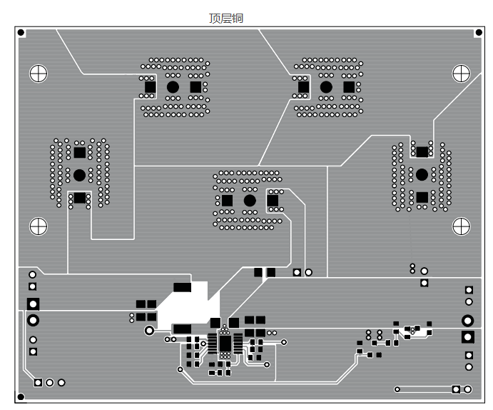
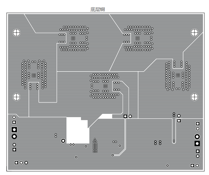
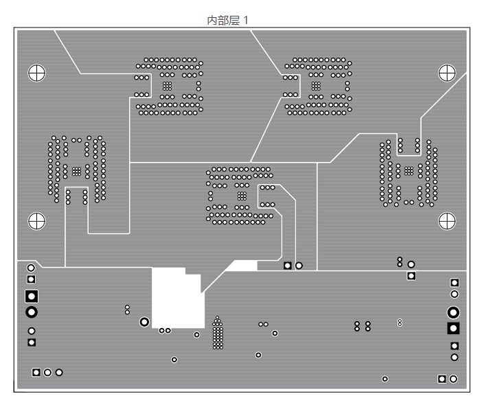
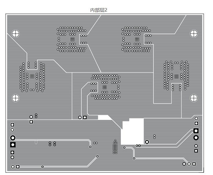
3. Board Layout
This section provides the board layout of the TPS61500EVM-369. A 4-layer PCB was used to help with the thermal dissipation of the WLEDs. Even with the low thermal impedance from the WLEDs to the internal layers, the entire PCB acts as a heatsink and so the board and especially the WLEDs get very hot. The user must carefully design their system to handle the thermal challenges raised by the WLEDs.
Board layout is critical for all switch-mode power supplies. See the data sheet (SLVS893) for specific layout and routing guidelines.

4 Schematic and Bill of Materials
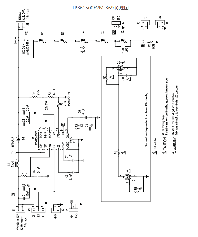
This section contains a schematic and bill of materials for the TPS61500EVM-369.
5.1 TPS61500EVM-369 Schematic
- LP8557IEVM_TI(德州仪器)中文资料_英文资料_价格_PDF手册
- LAUNCHXL-F28027F TI(德州仪器)中文资料_英文资料_价格_PDF手册
- DLPDLCR160CPEVM DLP160CP TI(德州仪器)中文资料_英文资料_价格_PDF手册
- THS4631DDAEVM TI(德州仪器)中文资料_英文资料_价格_PDF手册
- DAC3482EVM TI(德州仪器)中文资料_英文资料_价格_PDF手册
- THS4302EVM TI(德州仪器)中文资料_英文资料_价格_PDF手册
- ADS7038Q1EVM-PDK_TI(德州仪器)中文资料_英文资料_价格_PDF手册
- LM3450AEV230V30/NOPB_TI(德州仪器)中文资料_英文资料_价格_PDF手册
- TPS72728DSEEVM-406_TI(德州仪器)中文资料_英文资料_价格_PDF手册
- WL1835MODCOM8A_TI(德州仪器)中文资料_英文资料_价格_PDF手册
- TAS5424BQ1DKDEVM_TI(德州仪器)中文资料_英文资料_价格_PDF手册
- ADS7042EVM-PDK_TI(德州仪器)中文资料_英文资料_价格_PDF手册
- TMDS570LS31HDK_TI(德州仪器)中文资料_英文资料_价格_PDF手册
- VCA8500BOARD_TI(德州仪器)中文资料_英文资料_价格_PDF手册
- DEM-SOT223LDO_TI(德州仪器)中文资料_英文资料_价格_PDF手册
