This user's guide describes the characteristics, operation, and use of the ADS8402/ADS8406/ADS8412 16-bit, high-speed, parallel interface, analog-to-digital converter evaluation board. A complete circuit description, schematic diagram, and bill of materials are included.
1 EVM Overview
1.1 Features
• Full-featured evaluation board for the ADS8402 (1.25 MHz), ADS8406 (1.25 MHz), and ADS8412 (2 MHz) high-speed 16-bit, single channel, parallel interface SAR-type analog-to-digital converters.
• Onboard Signal Conditioning
• Onboard Reference
• Input and Output Digital Buffers
• Onboard Decoding for Stacking Multiple EVMs
2 Analog Interface
The ADS8402/ADS8406/ADS8412EVM analog-to-digital converter has pseudo-bipolar differential input. A pseudo-bipolar differential input is a differential signal (inverting and noninverting input is 180 degrees out of phase) that is level shifted such that the signals levels are always equal to or above zero volts. The peak-to-peak amplitude on each input pin can be as large as the reference voltage. See the respective product data sheet for more information.
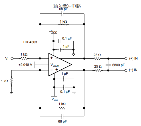
The ADS8402/ADS8406/ADS8412EVM comes installed with the unity gain buffer (U2) wired for single-ended into differential-out configuration. The common-mode voltage is derived from REF3040 reference IC and adjustable using a potentiometer (R9). The common mode voltage pin of the THS4503 is set to 2.0 V on the evaluation module. A single-ended input signal can be applied at pin-connector P1 or via SMA connectors J2 (noninverting input). The buffer circuit can be reconfigured for a differential input by installing resistor R6 and R8 and removing R1. The inverting leg of the differential signal should be applied to either connector P1 pin 1 or SMA connector J4 (inverting input). See Table 1 for pinout of analog connector, P1. See Section 8 for the EVM schematic.
2.1 Signal Conditioning
It is recommended that the analog input to any SAR-type converter be buffered. The amplifier circuit in Figure 1 is the buffer circuit used on the ADS8402/ADS8406/ADS8412EVM. This circuit consists of the THS4503, a high-speed fully differential amplifier configured as a single-ended into differential-out, unity gain buffer. The circuit shown in Figure 1 was optimized to achieve the ac (i.e., SNR, THD, SFDR, etc) specifications listed in the ADS8402, ADS8406, and ADS8412 data sheets. The 68-pF and 6800-pF capacitors in the signal path are polypropylene type, manufactured by WIMA Corporation. Polypropylene capacitors cause the least distortion of the input signal; therefore, they provide good dynamic performance from the converter. A low-cost alternative for the polypropylene type are C0G capacitors by TDK Corporation.

2.2 Reference
The EVM allows users to select from three reference sources. The ADS8402/ADS8406/ADS8412EVM provides an onboard 4.096-V reference, U3. The EVM also has the provision for users to supply a reference voltage via connector P1 pin 20. The user reference voltage and onboard reference voltages can be filtered by installing amplifier U1. The ADS8402, ADS8406, and ADS8412 analog-to-digital converters have a integrated onboard reference buffer; therefore, it is not necessary to buffer the voltage externally. The reference buffer circuit on the EVM is not populated with an amplifier for this reason. The EVM comes installed with on-chip internal reference tied directly to the reference pin of the converter. See Section 8 for a full schematic.
3 Digital Interface
The ADS8402/ADS8406/ADS8412 EVM is designed for easy interfacing to multiple platforms. Samtec part numbers SSW-110-22-F-D-VS-K and TSM-110-01-T-DV-P provide a convenient dual-row header/socket combination at P2 and P3. Consult Samtec at www.samtec.com or 1-800-SAMTEC-9 for a variety of mating connector options.
Read (RD), conversion start (CONVST) and reset (RESET) signals to the converter can be assigned to two different addresses in memory via jumper settings. This allows for the stacking of up to two ADS8402EVM, ADS8406EVM, and/or ADS8412EVMs into processor memory. See Table 4 for jumper settings. Note that the evaluation module does not allow the chip select ( CS) line of the converter to be assigned to different memory locations. It is therefore suggested that the CS line be grounded or wired to an appropriate signal of the processor.
- LP8557IEVM_TI(德州仪器)中文资料_英文资料_价格_PDF手册
- LAUNCHXL-F28027F TI(德州仪器)中文资料_英文资料_价格_PDF手册
- DLPDLCR160CPEVM DLP160CP TI(德州仪器)中文资料_英文资料_价格_PDF手册
- THS4631DDAEVM TI(德州仪器)中文资料_英文资料_价格_PDF手册
- DAC3482EVM TI(德州仪器)中文资料_英文资料_价格_PDF手册
- THS4302EVM TI(德州仪器)中文资料_英文资料_价格_PDF手册
- ADS7038Q1EVM-PDK_TI(德州仪器)中文资料_英文资料_价格_PDF手册
- LM3450AEV230V30/NOPB_TI(德州仪器)中文资料_英文资料_价格_PDF手册
- TPS72728DSEEVM-406_TI(德州仪器)中文资料_英文资料_价格_PDF手册
- WL1835MODCOM8A_TI(德州仪器)中文资料_英文资料_价格_PDF手册
- TAS5424BQ1DKDEVM_TI(德州仪器)中文资料_英文资料_价格_PDF手册
- ADS7042EVM-PDK_TI(德州仪器)中文资料_英文资料_价格_PDF手册
- TMDS570LS31HDK_TI(德州仪器)中文资料_英文资料_价格_PDF手册
- VCA8500BOARD_TI(德州仪器)中文资料_英文资料_价格_PDF手册
- DEM-SOT223LDO_TI(德州仪器)中文资料_英文资料_价格_PDF手册
