DAC8564EVM
This user’s guide describes the characteristics, operation, and the use of the DAC8564/65 evaluation module. It covers all pertinent areas involved to properly use this EVM board along with the devices that it supports. The physical PCB layout, schematic diagram, and circuit descriptions are included.
1 EVM Overview
This section gives a general overview of the DAC8564/65 evaluation module (EVM) and describes some of the factors that must be considered in using this module.
1.1 Features
This EVM features the DAC8564 or the DAC8565 digital-to-analog converters (DAC). The DAC8564/65EVM is a simple evaluation module designed as a quick and easy way to evaluate the functionality and performance of the 16-bit high-resolution, quad-channel, and serial input DAC with a built-in 2.5-V internal reference that is enabled by default. This EVM features a serial interface to communicate with any host microprocessor or TI DSP-based system.
Although the DAC was designed for single-supply operation, a bipolar output range is also possible by properly configuring the output operational amplifier, U2, circuit. This is discussed in detail in section 3.2.3. In addition, the external operational amplifier is also installed as an option to provide output signal conditioning or boost capacitive load drive and for other output mode requirement desired. The external output operational amplifier only supports one DAC output at a time.
A +5-V precision voltage reference is provided via U3 as well as a provision to apply user’s choice of reference supply via TP2 and TP3 test points. These reference supplies are optional voltage references provided externally in case it is necessary to evaluate the DAC8564/65 with external reference circuits. The external +5-V reference source for VREFH can be selected via JMP8 jumper configuration.
The EVM also has a provision for possibly experimenting with different circuit loads on the reference of the DAC8564/65. These are available through R25 and C14.
1.2 Power Requirements
The following sections describe the power requirements of this EVM.
1.2.1 Supply Voltage
The DC power supply requirement for this DAC8564/65EVM (AVDD and IOVDD) is selectable between +3.3 V and +5 V via jumper headers (JMP7 and JMP17). The AVDD supply of +3.3 VA comes from J3A-8 whereas the +5 VA comes from J3A-3 terminal. The IOVDD supply of +3.3 VD comes from J3A-9 whereas the +5 VD comes from J3A-10 terminal. These power supply voltages are referenced to ground through the J3A-6 and J3A-5 terminals, respectively. The VCC and VSS supplies are only used by the U2 and U4 operational amplifiers as well as the U3 voltage reference, which ranges from +15 V to –15 V maximum and connects through J3A-1 and J3A-2 terminals, respectively. All the analog power supplies are referenced to analog ground through J3A-6 terminal.
The negative rail of the output operational amplifier, U2, can be selected between VSS and AGND via JMP10 jumper. The external operational amplifier is installed as an option to provide output signal conditioning or for other output mode requirement that is desired by the user.
1.2.2 Reference Voltage
The DAC8564/65 is equipped with a +2.5-V internal reference that is enabled by default. The +2.5-V internal reference can be measured from its VREFH pin, which can be used to source other devices that requires +2.5-V reference. Because the DAC8564/65’s internal reference is enabled by default, care should be taken to ensure that the JMP8 is open and JMP9 is shorted between pins 1 and 2. Otherwise, inaccurate performance or damage to the part can result. Provided that the external voltage that is applied to the VREFH pin does not exceed the applied voltage in the VDD pin, and it does not exceed 100 mA of sourcing current, the DAC8564/65 should not be damaged. It is not recommended to leave the external voltage applied on the VREFH pin if the internal reference is not disabled. The external reference source must be disconnected immediately and the EVM power must be recycled to ensure the correct performance of the device.
The +5-V precision voltage reference is provided as an optional reference source to supply the external voltage reference for the DAC through REF02, U3. This reference voltage is selectable via jumper, JMP8. When shorting pins 1 and 2, the +5-V reference is selected whereas shorting pins 2 and 3 selects user preferred reference. The jumper, JMP9 must be shorted between pins 1 and 2 in order for the VREFL pin of the DAC to be properly grounded
The +5-V reference voltage goes through an adjustable 100-kΩ potentiometer, R15, in series with 20-kΩ R16, to allow the user to adjust the reference voltage to its desired settings. The voltage reference is then buffered through U4A as seen by the device under test. The REF02 precision reference is powered by VCC (+15 V) through J3A-1 terminal.
1.3 EVM Basic Functions
This EVM is designed primarily as a functional evaluation platform to test certain functional characteristics of the DAC8564/65 digital-to-analog converter. Functional evaluation of the installed DAC device can be accomplished with the use of any microprocessor, TI DSP, or a signal/waveform generator.
The headers J2A (top side) and J2B (bottom side) are pass-through connectors provided to allow the control signals and data required to interface a host processor or waveform generator to the DAC8564/65EVM using a custom-built cable
An adapter interface board (5-6k adapter interface) is also available to fit and mate with TI’s C5000™ and C6000™ DSP Starter Kit (DSK). This makes it unnecessary to build a custom cable. In addition, the Precision Analog Application group of Texas Instruments has other interface boards that are designed to connect to and interface with this EVM as well. For more details or information regarding the 5-6k adapter interface board or the other interface platforms.
The DAC outputs can be monitored through the selected pins of J4A header connector. The outputs can be switched through each of their respective jumpers, JMP11, JMP12, JMP13, and JMP14 for the stacking purposes. The stacking of multiple EVMs allows a total of eight (DAC8564/65) DAC channels to be used provided that the frame synchronization signal, SYNC, is unique for each EVM board stacked. The SYNC signal can be selected for each EVM board via jumper JMP18.
addition, the option of selecting the DAC output to be fed to the non-inverting side of the output operational amplifier, U2, is also possible by using a jumper across the selected pins of J4A. The output operational amplifier, U2, must be first configured correctly for the desired waveform characteristic (see section 3 of this user’s guide manual).
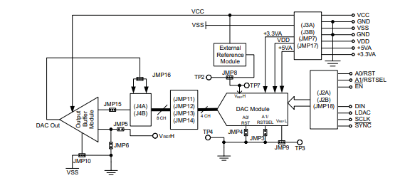
A block diagram of the EVM is shown in Figure 1.
2 PCB Design and Performance
This section talks about the layout design of the PCB thereby describing the physical and mechanical characteristics of the EVM, as well as a brief description of the EVM test performance procedure performed. The list of components used on this evaluation module is also included in this section.
2.1 PCB Layout
The DAC8564/65 EVM is designed to preserve the performance quality of the DAC, device under test, as specified in the data sheet. Carefully analyzing the EVM’s physical restrictions and the given or known elements that contributes to the EVM’s performance degradation is the key to a successful design implementation. These obvious attributes that diminish the performance of the EVM can be easily addressed during the schematic design phase, by properly selecting the right components and building the circuit correctly. The circuit must include adequate bypassing, identifying and managing the analog and digital signals, and understanding the components mechanical attributes.
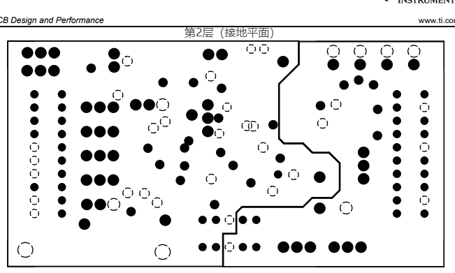
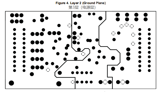
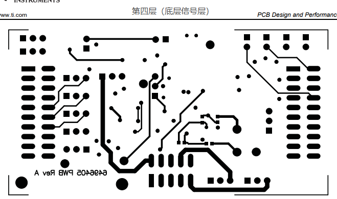
The obscure part of the design is the layout process in which limited knowledge and inexperience can easily present a problem. The main concern is primarily with component placement and the proper routing of signals. The bypass capacitors must be placed as close as possible to the pins, and the analog and digital signals must be properly separated from each other. The power and ground plane is very important and must be carefully considered in the layout process. A solid plane is ideally preferred but sometimes impractical. Therefore, when solid planes are not possible, a split plane does the job as well. When considering a split plane design, analyze the component placement and carefully split the board into its analog and digital sections starting from the device under test. The ground plane plays an important role in controlling the noise and other effects that otherwise contributes to the error of the DAC output. To ensure that the return currents are handled properly, route the appropriate signals only in their respective sections, meaning that the analog traces should only lay directly above or below the analog section and the digital traces in the digital section. Minimize the length of the traces but use the biggest possible trace width allowable in the design. These design practices discussed can be seen in the following illustrations
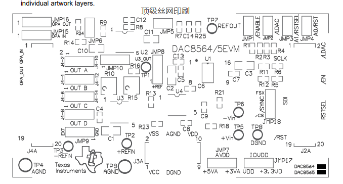
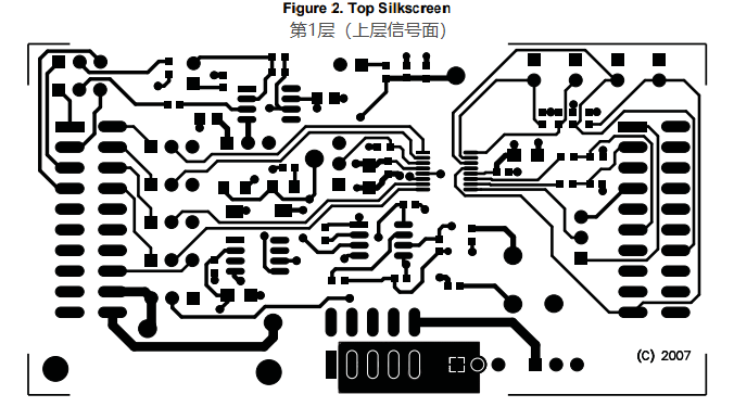
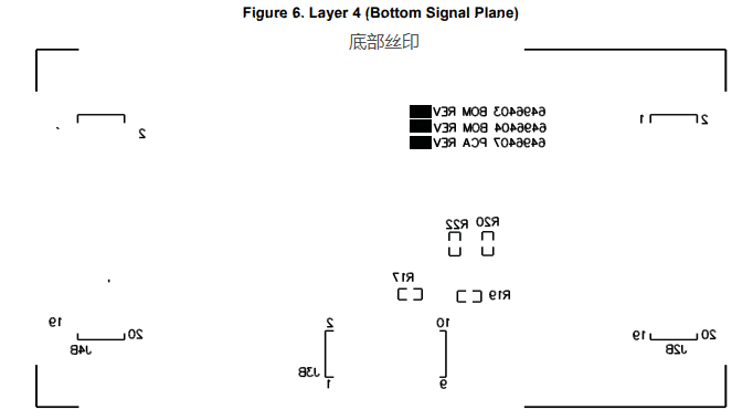
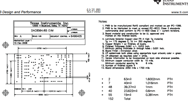
The DAC8564/65EVM board is constructed on a four-layer printed-circuit board using a copper-clad FR-4 laminate material. The printed-circuit board has a dimension of 43,1800 mm (1.7000 inch) × 82,5500 mm (3.2500 inch), and the board thickness is 1,5748 mm (0.062 inch). Figure 2 through Figure 8 show the individual artwork layers.
- LP8557IEVM_TI(德州仪器)中文资料_英文资料_价格_PDF手册
- LAUNCHXL-F28027F TI(德州仪器)中文资料_英文资料_价格_PDF手册
- DLPDLCR160CPEVM DLP160CP TI(德州仪器)中文资料_英文资料_价格_PDF手册
- THS4631DDAEVM TI(德州仪器)中文资料_英文资料_价格_PDF手册
- DAC3482EVM TI(德州仪器)中文资料_英文资料_价格_PDF手册
- THS4302EVM TI(德州仪器)中文资料_英文资料_价格_PDF手册
- ADS7038Q1EVM-PDK_TI(德州仪器)中文资料_英文资料_价格_PDF手册
- LM3450AEV230V30/NOPB_TI(德州仪器)中文资料_英文资料_价格_PDF手册
- TPS72728DSEEVM-406_TI(德州仪器)中文资料_英文资料_价格_PDF手册
- WL1835MODCOM8A_TI(德州仪器)中文资料_英文资料_价格_PDF手册
- TAS5424BQ1DKDEVM_TI(德州仪器)中文资料_英文资料_价格_PDF手册
- ADS7042EVM-PDK_TI(德州仪器)中文资料_英文资料_价格_PDF手册
- TMDS570LS31HDK_TI(德州仪器)中文资料_英文资料_价格_PDF手册
- VCA8500BOARD_TI(德州仪器)中文资料_英文资料_价格_PDF手册
- DEM-SOT223LDO_TI(德州仪器)中文资料_英文资料_价格_PDF手册
